We propose several possible physical causes for the above phenomena as follows:
 -type low-doped
silicon (
-type low-doped
silicon ( ) the effect becomes
important at surface fields higher than
) the effect becomes
important at surface fields higher than  at room
temperature [136]. These effects have been investigated in
detail in [453] for high field strengths and doping levels,
employing the rigorous model from [452]. Differences between
the surface potential calculated classically and quantum mechanically
(QM) become quite large at very high oxide fields. For
at room
temperature [136]. These effects have been investigated in
detail in [453] for high field strengths and doping levels,
employing the rigorous model from [452]. Differences between
the surface potential calculated classically and quantum mechanically
(QM) become quite large at very high oxide fields. For
 , the surface band-bending are
 [453],
 and
and 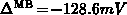 in
in
 -type gate with
  at
at  . At
lower doping
. At
lower doping  ,
,  ,
,
 and
and  at
the same field and temperature. Note that the results
denoted in [453] as classical solution, have been obtained
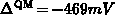
by MB statistics. When applying FD statistics for a three-dimensional
electron gas instead of MB statistics, the quantum-mechanical
correction is smaller, but still remains significant.
at
the same field and temperature. Note that the results
denoted in [453] as classical solution, have been obtained
by MB statistics. When applying FD statistics for a three-dimensional
electron gas instead of MB statistics, the quantum-mechanical
correction is smaller, but still remains significant.
 becomes comparable to the semiconductor capacitance - that means,
at thin oxides. In the case of -gate/-channel and
-gate/-channel devices, the lowering of semiconductor
capacitance in the accumulation due to quantum-mechanical effects
occurs at the same
time in both, gate and bulk leading to an enhanced deviation from the
classical theory. This could be the explanation for the very slow rise
of
becomes comparable to the semiconductor capacitance - that means,
at thin oxides. In the case of -gate/-channel and
-gate/-channel devices, the lowering of semiconductor
capacitance in the accumulation due to quantum-mechanical effects
occurs at the same
time in both, gate and bulk leading to an enhanced deviation from the
classical theory. This could be the explanation for the very slow rise
of  from depletion to heavy accumulation that is measured
on the -gate/-channel device with
from depletion to heavy accumulation that is measured
on the -gate/-channel device with  oxide.
curve, as demonstrated in
Figures 2.9, 2.11
and 2.12. With increasing  it is, however,
necessary to assume a higher amount of traps to explain the
experiments. In addition, we did not observe any significant
change in the
it is, however,
necessary to assume a higher amount of traps to explain the
experiments. In addition, we did not observe any significant
change in the  curve of -gate/-channel
devices when varying the signal from
curve of -gate/-channel
devices when varying the signal from  kHz to MHz! Therefore, if
there are any traps at the gate/oxide interface, their repopulation
must be very fast. An additional conclusion is that the minority
carriers can invert very quickly in the gate in our
-gate/-channel devices. We observed that an opposite effect has
been measured in a lightly doped -type gate
in [367]
kHz to MHz! Therefore, if
there are any traps at the gate/oxide interface, their repopulation
must be very fast. An additional conclusion is that the minority
carriers can invert very quickly in the gate in our
-gate/-channel devices. We observed that an opposite effect has
been measured in a lightly doped -type gate
in [367] . An evident finite time
response of minority carriers in the gate is measured in
-gate/-channel
devices in [226] and [269]. Whether the differences
between gate-types regularly appear and why is not clear at present.
A smooth inversion in the gate may come out as an artifact in
measurements when the AC signal is high, due to finite time response
of minorities [269]. For the characteristics in
Figure 2.9 we, however, did not observe an
. An evident finite time
response of minority carriers in the gate is measured in
-gate/-channel
devices in [226] and [269]. Whether the differences
between gate-types regularly appear and why is not clear at present.
A smooth inversion in the gate may come out as an artifact in
measurements when the AC signal is high, due to finite time response
of minorities [269]. For the characteristics in
Figure 2.9 we, however, did not observe an
 -dependence.
 -
- curve may be related to traps at
the grain boundaries residing at the polysilicon/oxide interface.
The typical density of grain interface sites is of the order
curve may be related to traps at
the grain boundaries residing at the polysilicon/oxide interface.
The typical density of grain interface sites is of the order
 , which is comparable with that assumed to
fit the experiment. In addition, if the first layer in the
polysilicon close to the interface is built of very small grains, the
equivalent volume trap density
, which is comparable with that assumed to
fit the experiment. In addition, if the first layer in the
polysilicon close to the interface is built of very small grains, the
equivalent volume trap density  can be very large
close to the interface and can no longer be neglected compared to
. A significant trapping of majority carriers takes place just
at the interface leading to formation of a shallow resistive layer.
Our knowledge of the polysilicon-gate structure in the very first
can be very large
close to the interface and can no longer be neglected compared to
. A significant trapping of majority carriers takes place just
at the interface leading to formation of a shallow resistive layer.
Our knowledge of the polysilicon-gate structure in the very first
 from the gate/oxide interface is quite indigent at
present, although some studies may be found in the
literature [6].
from the gate/oxide interface is quite indigent at
present, although some studies may be found in the
literature [6].
 from the gate/oxide interface
towards the gate-body can explain a low slope in the
from the gate/oxide interface
towards the gate-body can explain a low slope in the  versus
 curve. However, the region of interest is very shallow. The
depletion region in the gate becomes only
curve. However, the region of interest is very shallow. The
depletion region in the gate becomes only  at
at  for device in Figure 2.9. Note that the distance
between impurity atoms is
for device in Figure 2.9. Note that the distance
between impurity atoms is  on the average at this doping level
(
on the average at this doping level
( ). To explain the experiment in
Figure 2.9 should be assumed to
increase within the first
). To explain the experiment in
Figure 2.9 should be assumed to
increase within the first  from the interface in this
device. After becoming fully depleted at a moderate
from the interface in this
device. After becoming fully depleted at a moderate  ,
this shallow low-doped region acts as a constant
,
this shallow low-doped region acts as a constant  at a higher
. A further increase in
at a higher
. A further increase in  is proportional
to
is proportional
to  , but not to
  as it is for constant doping.
Contrary to our erroneous conclusion in [167] the analytical
modeling confirmed with numerical simulation has shown that a
nonuniform dopant distribution can explain well the smooth inversion
in the gate, when the transition region for is very shallow
and the doping level in the gate-body is high.
as it is for constant doping.
Contrary to our erroneous conclusion in [167] the analytical
modeling confirmed with numerical simulation has shown that a
nonuniform dopant distribution can explain well the smooth inversion
in the gate, when the transition region for is very shallow
and the doping level in the gate-body is high.
 may have an impact on the
- characteristics. To confirm this hypothesis we assume that
the large-area device consists of many non-interacting small devices
in parallel, each of them with a constant dopant concentration in the
gate. This approach is known as the parallel array model, already
applied in several similar analyses [331]. The impurity
concentration is different in each particular small device,
with an average value of
may have an impact on the
- characteristics. To confirm this hypothesis we assume that
the large-area device consists of many non-interacting small devices
in parallel, each of them with a constant dopant concentration in the
gate. This approach is known as the parallel array model, already
applied in several similar analyses [331]. The impurity
concentration is different in each particular small device,
with an average value of  across the large device.
Considering a physically small volume
across the large device.
Considering a physically small volume  , the number of dopant atoms
contained in becomes
, the number of dopant atoms
contained in becomes  . In the constant volume ,
 obeys the Poisson distribution, as for example interface point
charges do [331], with mathematical expectation of
obeys the Poisson distribution, as for example interface point
charges do [331], with mathematical expectation of
 and standard deviation of
 . It follows the standard
deviation of the dopant concentration
. It follows the standard
deviation of the dopant concentration
 .
For a sufficiently large that
.
For a sufficiently large that  holds, may be
well approximated by a gaussian distribution as is done in our
calculations.
In each single device the gate charge
holds, may be
well approximated by a gaussian distribution as is done in our
calculations.
In each single device the gate charge  and the surface potential
are calculated by the selfconsistent one-dimensional
analytical model introduced in Section 2.2,
for chosen randomly. The result for the large-area device
follows after building the statistical averages. The choice of is
discussed briefly. We assume
and the surface potential
are calculated by the selfconsistent one-dimensional
analytical model introduced in Section 2.2,
for chosen randomly. The result for the large-area device
follows after building the statistical averages. The choice of is
discussed briefly. We assume  , where
 is the depletion region width at the doping level .
For the parallel array model to be reasonable
is the depletion region width at the doping level .
For the parallel array model to be reasonable  must be
larger than
must be
larger than  :
:  , with parameter
  .
If is fixed as interesting for the onset of gate inversion,
it follows
.
If is fixed as interesting for the onset of gate inversion,
it follows  .
In depletion, can be considered as constant and we obtain
.
In depletion, can be considered as constant and we obtain
 . In both cases
the relative standard deviation
. In both cases
the relative standard deviation  increases with increasing doping level . For example
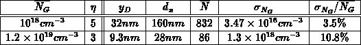
 is assumed in the calculation.
The second example corresponds to
is assumed in the calculation.
The second example corresponds to
Figure 2.9. A  large-area
device contains
large-area
device contains  small devices in the latter case.
Let us consider the total depletion in the gate. Moving carriers are
neglected. The surface electric field governed by the oxide
field  is negligibly influenced by variations in ,
because of
is negligibly influenced by variations in ,
because of  . We omit
  from discussion. The
gate capacitance in depletion is related to by
from discussion. The
gate capacitance in depletion is related to by
 . Therefore, becomes approximately
gaussian distributed as well. For the bulk capacitance
. Therefore, becomes approximately
gaussian distributed as well. For the bulk capacitance  in 2.23,
  holds on the
inversion side of the - curve. Thereby, the gate capacitance
becomes
holds on the
inversion side of the - curve. Thereby, the gate capacitance
becomes  which
can be further approximated by
which
can be further approximated by 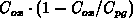 , valid
if
, valid
if  . Simple analytical considerations lead to
 , where the line over the
quantity denotes the mathematical expectation. Similarly, for the
surface potential in depletion
, where the line over the
quantity denotes the mathematical expectation. Similarly, for the
surface potential in depletion
 one obtains
 . We have exploited
the inequality
. We have exploited
the inequality  , valid for a random
variable
, valid for a random
variable  which is gaussian distributed. Therefore, the statistical
variations in the gate doping not only induce fluctuations in
across the large device, but also increase the mean value
of and lower the mean value of measured on a large
device. A similar result has been obtained by numerical simulation of
the effect of bulk doping fluctuations on the threshold voltage of
small MOSFETs in [339]. The slight changes of and
in depletion region following from analytical
considerations are completely in coherence with results from
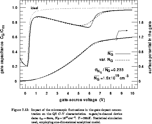
statistical simulations, Figure 2.13.
which is gaussian distributed. Therefore, the statistical
variations in the gate doping not only induce fluctuations in
across the large device, but also increase the mean value
of and lower the mean value of measured on a large
device. A similar result has been obtained by numerical simulation of
the effect of bulk doping fluctuations on the threshold voltage of
small MOSFETs in [339]. The slight changes of and
in depletion region following from analytical
considerations are completely in coherence with results from
statistical simulations, Figure 2.13.
More important than small changes occurring in the gate depletion is
the impact of the point fluctuations of dopants on inversion at the
gate/oxide interface. Let us assume . It
follows  for the Debye length at . A
parallelopiped with
for the Debye length at . A
parallelopiped with  base and
  height (comparable with the depth of depleted region) contains only
 dopant atoms on average, namely there are
  atoms in
the first
atoms in
the first  from the gate/oxide interface. Any macroscopic
approach to and space charge density is no longer valid with
respect to the carrier concentrations. Model-calculations accounting
for the dopant fluctuations and experiments have shown that the
stretch-out of the gate-channel capacitance of MOS-system already
takes place at a bulk doping of
from the gate/oxide interface. Any macroscopic
approach to and space charge density is no longer valid with
respect to the carrier concentrations. Model-calculations accounting
for the dopant fluctuations and experiments have shown that the
stretch-out of the gate-channel capacitance of MOS-system already
takes place at a bulk doping of  at room
temperature [504] (see also [506]). The same effect
occurs in the gate-channel capacitance associated with the gate
(minority carrier component in on the inversion side),
producing a stretch-out in as well. This effect has been at
least qualitatively reproduced in our statistical simulations shown
in Figure 2.13, in comparison with experimental
data for similar devices. Moreover, by increasing the dopant
concentration , the gate-channel capacitance becomes
smoother. This fact can qualitatively explain Fig.1 in [281],
which shows a fast inversion in the low-doped gate and a smooth
recovery for the heavy-doped one. Finally, we think the random
distribution of dopants in a shallow depleted region close to the
gate/oxide interface is an obvious explanation for the smooth
inversion in heavily doped gates [167].
at room
temperature [504] (see also [506]). The same effect
occurs in the gate-channel capacitance associated with the gate
(minority carrier component in on the inversion side),
producing a stretch-out in as well. This effect has been at
least qualitatively reproduced in our statistical simulations shown
in Figure 2.13, in comparison with experimental
data for similar devices. Moreover, by increasing the dopant
concentration , the gate-channel capacitance becomes
smoother. This fact can qualitatively explain Fig.1 in [281],
which shows a fast inversion in the low-doped gate and a smooth
recovery for the heavy-doped one. Finally, we think the random
distribution of dopants in a shallow depleted region close to the
gate/oxide interface is an obvious explanation for the smooth
inversion in heavily doped gates [167].
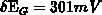
- characteristics of MOS
capacitors with bulk doped heavily is measured and modeled. A very
large total band-gap narrowing  was
necessary to fit the minimum of high-frequency on the inversion
side when the rigid-parabolic-band model with constant band-gap
narrowing is assumed. For example: the extracted values
was
necessary to fit the minimum of high-frequency on the inversion
side when the rigid-parabolic-band model with constant band-gap
narrowing is assumed. For example: the extracted values
 and
and  are much higher than the
values of about
are much higher than the
values of about  and
and  for the electrical band-gap
narrowing in the quasi-neutral regions at
for the electrical band-gap
narrowing in the quasi-neutral regions at
 and
and  ,
respectively. These large values are in accord with the theoretical
predictions in [280].
becomes lower comparing with the rigid-parabolic-band model. Thereby,
we expect lowering of in the weak gate depletion. In stronger
depletion, the discussion in 5) holds. At high the
minority carriers begin to fill the deep states in the corresponding
opposite tail. As a consequence, an overall slope of the
curve is reduced on the inversion side of the
characteristics. In addition, filling of deep band states by
minorities leads to a smooth inversion in the gate. The latter effect
has been heuristically reproduced by interface traps in
Figures 2.9, 2.11
and 2.12.
,
respectively. These large values are in accord with the theoretical
predictions in [280].
becomes lower comparing with the rigid-parabolic-band model. Thereby,
we expect lowering of in the weak gate depletion. In stronger
depletion, the discussion in 5) holds. At high the
minority carriers begin to fill the deep states in the corresponding
opposite tail. As a consequence, an overall slope of the
curve is reduced on the inversion side of the
characteristics. In addition, filling of deep band states by
minorities leads to a smooth inversion in the gate. The latter effect
has been heuristically reproduced by interface traps in
Figures 2.9, 2.11
and 2.12.