The model 2.7 based on parabolic band, with constant
band-gap narrowing  and
and  assumed
in 2.9, is used in comparison with experimental results. An
important assumption in this model is that the conduction and valence band
shifts depend solely on the activated impurity concentration
assumed
in 2.9, is used in comparison with experimental results. An
important assumption in this model is that the conduction and valence band
shifts depend solely on the activated impurity concentration  , but not on
carrier concentrations which vary with potential. The total gap narrowing
, but not on
carrier concentrations which vary with potential. The total gap narrowing
 is modeled with an empirical expression A.25 in
Appendix A, which correlates with experimental data for electrical
gap narrowing in quasi-neutral regions from literature. Such a model is
successfully used in device modeling, e.g. in modeling diodes and
bipolar transistors [327][315][190], JFET's [317] and solar
cells [316]. We will study whether this approach is appropriate for
modeling heavily doped depleted regions. In the absence of any experimental data
in literature, symmetrical narrowing is assumed:
is modeled with an empirical expression A.25 in
Appendix A, which correlates with experimental data for electrical
gap narrowing in quasi-neutral regions from literature. Such a model is
successfully used in device modeling, e.g. in modeling diodes and
bipolar transistors [327][315][190], JFET's [317] and solar
cells [316]. We will study whether this approach is appropriate for
modeling heavily doped depleted regions. In the absence of any experimental data
in literature, symmetrical narrowing is assumed:
 .
.
To calculate the theoretical  -
- characteristics we used MINIMOS,
because of nonuniform bulk doping in test MOSFETs. A constant is
assumed in the gate area.
characteristics we used MINIMOS,
because of nonuniform bulk doping in test MOSFETs. A constant is
assumed in the gate area.
Integral quantities like inversion-layer charge density  , bulk surface
field
, bulk surface
field  and drain current are less influenced by an error in the gate model
than are differential quantities like gate capacitance
and drain current are less influenced by an error in the gate model
than are differential quantities like gate capacitance  . Actually, the
deviation of the quasi-static (QS) capacitance from experiment could be a direct
sense for an inaccuracy in the space-charge model and/or interface trap model
as explained later. Therefore, we choose the QS - characteristics
to compare the calculations with experimental results. Several
. Actually, the
deviation of the quasi-static (QS) capacitance from experiment could be a direct
sense for an inaccuracy in the space-charge model and/or interface trap model
as explained later. Therefore, we choose the QS - characteristics
to compare the calculations with experimental results. Several
 -gate/-channel devices
with oxide thickness
-gate/-channel devices
with oxide thickness  ,
,  ,
,  ,
,  and
and  and
two
and
two  -gate/-channel devices with
  and
and  are
examined
are
examined . One comparison between numerically
calculated and experimental QS - characteristics is given in
Figures 2.9 and 2.10. Capacitances are
measured by the split - technique [256]. Both measured,
gate-channel
. One comparison between numerically
calculated and experimental QS - characteristics is given in
Figures 2.9 and 2.10. Capacitances are
measured by the split - technique [256]. Both measured,
gate-channel  and gate-bulk
  capacitances are corrected due to
gate/source and gate/drain junction overlap capacitances and parasitic wiring
capacitances.
capacitances are corrected due to
gate/source and gate/drain junction overlap capacitances and parasitic wiring
capacitances.
The total capacitance is the sum of the corrected values
 . From maximal in strong accumulation it
follows
. From maximal in strong accumulation it
follows  , where
 is the channel width and
  is the corresponding effective
channel length. For an accurate comparison between theory and experiment it is
important to estimate properly the physical oxide thickness; the extracted
is the corresponding effective
channel length. For an accurate comparison between theory and experiment it is
important to estimate properly the physical oxide thickness; the extracted
 must provide for
  a value higher
than the highest value
measured at the strongest-accumulation point. It is known that, due to quantum
mechanical effects in accumulation layers, physical is always smaller
than that corresponding to maximal in experiments [453]. This
effect becomes quite significant for oxides thinner than
a value higher
than the highest value
measured at the strongest-accumulation point. It is known that, due to quantum
mechanical effects in accumulation layers, physical is always smaller
than that corresponding to maximal in experiments [453]. This
effect becomes quite significant for oxides thinner than  . Note that
our aim is not to fit the - characteristic in the intermediate voltage
range, but to extract an eventual small deviation of the theory from experiment.
For the device in Figure 2.9 we estimate
. Note that
our aim is not to fit the - characteristic in the intermediate voltage
range, but to extract an eventual small deviation of the theory from experiment.
For the device in Figure 2.9 we estimate
 .
.
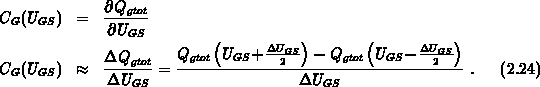
The QS gate capacitance, defined by 2.21, is calculated by MINIMOS applying the method [167]
 is the total charge in the gate including interface
states. It can be numerically obtained by calculating the flux of the electric
field through a contour in the oxide around the gate
(Figure 2.14). In applying 2.24 we used
is the total charge in the gate including interface
states. It can be numerically obtained by calculating the flux of the electric
field through a contour in the oxide around the gate
(Figure 2.14). In applying 2.24 we used
 ,
,  and froze the grid.
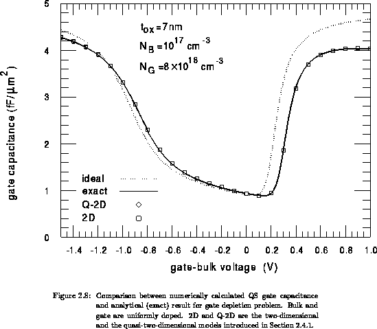
Comparing the numerical capacitance with the analytical results from
Section 2.2 for long-channel devices with uniformly
doped bulk we found this simple technique to be very accurate. One example is
demonstrated in Figure 2.8. The numerical error is small as
expected, whereas an influence of the discretization error is well suppressed
by using the same grid for both bias points,
and froze the grid.
Comparing the numerical capacitance with the analytical results from
Section 2.2 for long-channel devices with uniformly
doped bulk we found this simple technique to be very accurate. One example is
demonstrated in Figure 2.8. The numerical error is small as
expected, whereas an influence of the discretization error is well suppressed
by using the same grid for both bias points,  and
and
 .
.
For a comparison with the experiment we only include the field flux from the
source-subdiffusion to the drain-subdiffusion in calculating  , because
the fluxes in the gate/subdiffusion overlap region and the gate side-wall
fluxes which represent the parasitic overlap capacitances, have already been
subtracted from the experimental data. Moreover, numerical calculations show
that these parasitic capacitances are weakly bias-dependent from strong
accumulation to strong inversion, as usually assumed in the split -
technique. Therefore, it is confirmed that the assumption of constant parasitic
capacitances does not introduce a relevant error in our analysis.
, because
the fluxes in the gate/subdiffusion overlap region and the gate side-wall
fluxes which represent the parasitic overlap capacitances, have already been
subtracted from the experimental data. Moreover, numerical calculations show
that these parasitic capacitances are weakly bias-dependent from strong
accumulation to strong inversion, as usually assumed in the split -
technique. Therefore, it is confirmed that the assumption of constant parasitic
capacitances does not introduce a relevant error in our analysis.
The channel doping profile is obtained by fitting experimental  characteristics in bulk depletion from the minimum of the -
characteristics to the flat-band applying numerical simulation in 2-3 loops.
We neglected traps at the oxide/bulk interface and assumed for and
characteristics in bulk depletion from the minimum of the -
characteristics to the flat-band applying numerical simulation in 2-3 loops.
We neglected traps at the oxide/bulk interface and assumed for and
 the values determined below. The doping profile has a small influence
on the inversion side of the - characteristic far above the threshold,
which we focus on in the study. is estimated by matching simulated
with the experimental data at low effective-gate bias
the values determined below. The doping profile has a small influence
on the inversion side of the - characteristic far above the threshold,
which we focus on in the study. is estimated by matching simulated
with the experimental data at low effective-gate bias  . Higher
values enable better matching experimental data at a higher gate bias,
but worse
at lower . Arbitrarily assumed positive fixed charge at the
gate/oxide interface of
. Higher
values enable better matching experimental data at a higher gate bias,
but worse
at lower . Arbitrarily assumed positive fixed charge at the
gate/oxide interface of  improves the match with
measured
improves the match with
measured  (see Figure 2.9). At higher
the charge
(see Figure 2.9). At higher
the charge  has a minor impact on the -
characteristics. Regarding the band-gap shift
has a minor impact on the -
characteristics. Regarding the band-gap shift  , it has
a direct influence on the threshold voltage and the flat-band potential. The
impact of band-gap narrowing is very small, far above the threshold voltage.
, it has
a direct influence on the threshold voltage and the flat-band potential. The
impact of band-gap narrowing is very small, far above the threshold voltage.
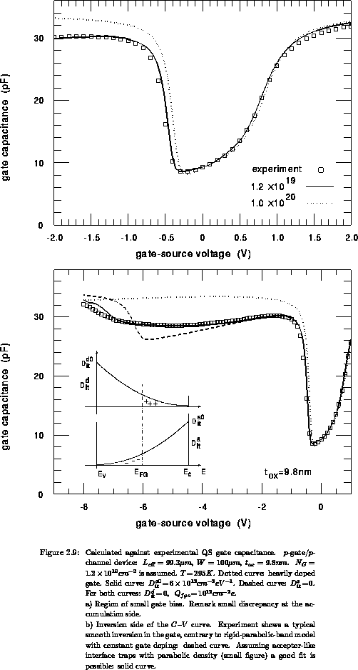
A comparison with measurements shown in Figure 2.9 clearly demonstrates that the capacitance resulting from the application of the rigid-parabolic-band model and constant doping near the gate/oxide interface (dashed curve) deviates from the experiment on the inversion side.
This disagreement between theory and experiment cannot be eliminated by
neither varying the gate doping , bulk doping nor the fixed charge at the
gate/oxide interface . The calculated slope of the - curve is
larger than the experimental one. Note that we have neglected all bulk,
grain-boundary and interface traps in the polysilicon in the calculation.
A second observation is that the inversion in the gate is smooth, while the
calculation shows a fast recovery of the gate capacitance to the
 limit for both, MB and FD statistics in the gate.
These findings may be an indication for inaccuracy in the space-charge and/or
interface-trap model in the gate. To understand this claim remember that the
relationship between the oxide field  and the surface potential in the
gate
and the surface potential in the
gate  reads
reads
in the general case.  is the space charge in the gate and is the
interface charge. The semiconductor capacitance
is the space charge in the gate and is the
interface charge. The semiconductor capacitance  in the gate including
interface traps is given by 2.23 resulting in
in the gate including
interface traps is given by 2.23 resulting in
The oxide field depends on the voltage drop in the oxide. When the gate
is doped moderately or heavily,  is much larger than in the
gate, as is the case in Figure 2.9 on the inversion side
of the characteristics. Therefore, is slightly influenced by an error
in
is much larger than in the
gate, as is the case in Figure 2.9 on the inversion side
of the characteristics. Therefore, is slightly influenced by an error
in  and
and  and may be considered as constant in
relationship 2.26 with respect to changes in the gate-model.
In addition, semiconductor capacitance in the bulk defined
by 2.23 is very large. As a consequence, deviations of
from experiment are exclusively due to , whereas this capacitance is
directly dependent on
and may be considered as constant in
relationship 2.26 with respect to changes in the gate-model.
In addition, semiconductor capacitance in the bulk defined
by 2.23 is very large. As a consequence, deviations of
from experiment are exclusively due to , whereas this capacitance is
directly dependent on  and
and  . At
the other hand, depends on by 2.25. We
may conclude that resulting from the rigid-parabolic-band model
with constant band-gap narrowing cannot explain the experimental results, if we
assume that the interface traps are not responsible for this finding.
. At
the other hand, depends on by 2.25. We
may conclude that resulting from the rigid-parabolic-band model
with constant band-gap narrowing cannot explain the experimental results, if we
assume that the interface traps are not responsible for this finding.
An evident engineering explanation that the nonuniform gate doping in direction perpendicular to the interface can account for these effects should be appreciated as well.
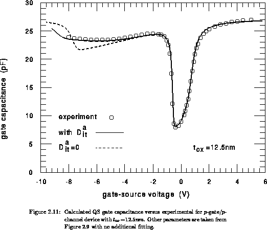
A simple engineering approach to improve fitting experimental data using the
present model is to assume acceptor-like traps at the gate/oxide interface in
-gate/-channel devices. In case of an -type gate donor-like traps
would have to be assumed. We found that acceptor-like traps with a parabolic
density in energy space
can satisfactorily reproduce our experimental data. In this model,  or
or  are the only variable parameters. All -gate/-channel
devices considered in this study have been fabricated with the same process,
except for the thickness of the final gate-oxide. We were able to fit all
- curves for different oxide thickness using the same value of
for an assumed constant and . For a
-gate/-channel device with the thickest gate oxide the result is shown
in Figure 2.11.
are the only variable parameters. All -gate/-channel
devices considered in this study have been fabricated with the same process,
except for the thickness of the final gate-oxide. We were able to fit all
- curves for different oxide thickness using the same value of
for an assumed constant and . For a
-gate/-channel device with the thickest gate oxide the result is shown
in Figure 2.11.
Differences between calculated and experimental capacitances can be observed on the accumulation side too; Figures 2.9 and 2.12. The experimental data lie below the calculated curve, although both characteristics match at flat-band and in the strong accumulation limit.
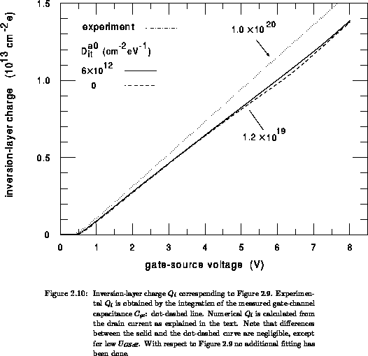
Comparison between inversion-layer charge densities corresponding to
Figures 2.9 is given in Figure 2.10.
Experimental per unit area is calculated by the numerical integration of
the experimental gate-channel capacitance  and dividing the
result with
and dividing the
result with  . Simulated is calculated from
the MINIMOS
drain current using the relation
. Simulated is calculated from
the MINIMOS
drain current using the relation  in the linear region. The dependence of
  on the transverse field has been
suppressed in the simulation. This has no influence on and because
the bulk is in quasi-equilibrium. The value of in the
active region near the interface is known exactly, as this is an input to the
simulation. This technique to calculate is simpler and more accurate than
the integration of
on the transverse field has been
suppressed in the simulation. This has no influence on and because
the bulk is in quasi-equilibrium. The value of in the
active region near the interface is known exactly, as this is an input to the
simulation. This technique to calculate is simpler and more accurate than
the integration of  across the channel used in [439][418]. For
comparison in Figure 2.10, no additional fitting has been
performed with respect to Figure 2.9. The agreement between
calculated and measured is very good, even without assuming traps at the
gate/oxide interface (dashed curve).
across the channel used in [439][418]. For
comparison in Figure 2.10, no additional fitting has been
performed with respect to Figure 2.9. The agreement between
calculated and measured is very good, even without assuming traps at the
gate/oxide interface (dashed curve).
In real devices, the error in  is smaller than the error in , as it
is discussed in more detail in Section 2.4.2. Let us
assume a positive error in due to an inaccuracy of the gate-model. This
error produces a positive error in and . The surface mobility
decreases due to a higher (at room temperature). The errors in
and partially compensate each other, leading to a smaller error
in the drain current
is smaller than the error in , as it
is discussed in more detail in Section 2.4.2. Let us
assume a positive error in due to an inaccuracy of the gate-model. This
error produces a positive error in and . The surface mobility
decreases due to a higher (at room temperature). The errors in
and partially compensate each other, leading to a smaller error
in the drain current  than in the channel-charge .
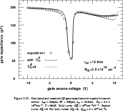
Measurements on -gate/-channel devices shown in
Figure 2.12 lead to the same conclusions as for
-gate/-channel devices. In addition, we analyzed several QS -
characteristics published in literature: Fig.1 and Fig.2 in [60],
Fig.5(a) in [512], Fig.1 in [281] and Fig.10 in [28].
Similar deviations are found. None of these data-sets can be reproduced
assuming the rigid-parabolic-band model and constant gate doping near the
interface. An inspection of the data shows that the observed phenomena are
reproducible and seem to be independent of the specific technological process
and of the type of gate ( or -type, polysilicon or amorphous silicon).
The observations are summarized below:
 is higher than the
experimental, although they match at flat-band and in the
limit.
is weakly dependent on
is higher than the
experimental, although they match at flat-band and in the
limit.
is weakly dependent on
 , while the calculated decreases strongly with
increasing .
recovers rapidly to
.
, while the calculated decreases strongly with
increasing .
recovers rapidly to
.