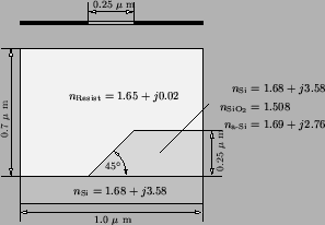
In all cases the simulation domain is
1.0 ![]() m x 1.0
m x 1.0 ![]() m x 0.7
m x 0.7 ![]() m large, and the
substrate material is silicon with a refractive index of
nSi = 1.68 + j3.58. For the nonplanar simulations a step
with a height of 0.25
m large, and the
substrate material is silicon with a refractive index of
nSi = 1.68 + j3.58. For the nonplanar simulations a step
with a height of 0.25 ![]() m and a slope of 45o is assumed to be
located in the middle of the simulation domain. The step material is either
dielectric oxide with a refractive index of
nSiO2 = 1.508 or
reflective a-silicon with a refractive index of
na-Si = 1.69 + j2.76. A non-bleaching DUV resist is chosen
with a refractive index of
nResist = 1.65 + j0.02. All
material parameters are taken from Table I of [6]. The mask
is situated in the center of the geometry, i.e., exactly above the slope,
and the mask-opening is 0.25
m and a slope of 45o is assumed to be
located in the middle of the simulation domain. The step material is either
dielectric oxide with a refractive index of
nSiO2 = 1.508 or
reflective a-silicon with a refractive index of
na-Si = 1.69 + j2.76. A non-bleaching DUV resist is chosen
with a refractive index of
nResist = 1.65 + j0.02. All
material parameters are taken from Table I of [6]. The mask
is situated in the center of the geometry, i.e., exactly above the slope,
and the mask-opening is 0.25 ![]() m x 0.25
m x 0.25 ![]() m wide.
A sketch of the investigated configuration is shown in
Figure 8.16.
m wide.
A sketch of the investigated configuration is shown in
Figure 8.16.
 |
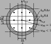
The stepper is a DUV projection printing system with a wavelength of 248 nm
and a fixed numerical aperture of
NA = 0.5. Three different
illumination apertures are compared, namely coherent, partially coherent or
circular with
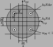
![]() = 0.8, and quadrupole with
= 0.8, and quadrupole with
![]() = 0.1 and X = Y = 0.7.
The number and location of the source points are illustrated in the discretized
wavevector diagram of Figure 8.17. The exposure dose
is set to 120 mJ/cm2 and the development time is chosen so that in all cases
the full contact is opened. For the resist an absorption parameter
of C = 0.013 cm2/mJ is assumed, and Kim's `R'-model is used
to calculate the development rate from the PAC concentration
(cf. Section 7.2.1). The `R'-parameter set is taken from
Table IV of [75]:
R1 = 0.25
= 0.1 and X = Y = 0.7.
The number and location of the source points are illustrated in the discretized
wavevector diagram of Figure 8.17. The exposure dose
is set to 120 mJ/cm2 and the development time is chosen so that in all cases
the full contact is opened. For the resist an absorption parameter
of C = 0.013 cm2/mJ is assumed, and Kim's `R'-model is used
to calculate the development rate from the PAC concentration
(cf. Section 7.2.1). The `R'-parameter set is taken from
Table IV of [75]:
R1 = 0.25 ![]() m/s,
R2 = 0.0005
m/s,
R2 = 0.0005 ![]() m/s, and
R3 = 7.4. All simulations are performed with ideal focus as well as
with a defocus of 1
m/s, and
R3 = 7.4. All simulations are performed with ideal focus as well as
with a defocus of 1 ![]() m above the resist surface.
m above the resist surface.
 |
For the simulation of the EM field propagation inside the simulation domain
51 Fourier modes in x-direction and 21 in y-direction
are used to represent the EM field. These values correspond to cut-off
frequencies of Nx = 25 and Ny = 10 applied to the differential method
(cf. Section 6.2.5).
The differential method thus consumes approximately 300 MB memory
(cf. Section 6.5.1). The number Nz
of discretization points is in the planar and dielectric cases 50, and in the
reflective case 75 since the stronger absorption in a-silicon has to be resolved
properly to obtain a stable performance of the stabilized march algorithm.
The run-times range between 4 to 5 hours on a DEC-600/333 workstation
depending on the step material. The development simulation is performed with a
cell density of 300 cells/![]() m. The memory usage is 20 MB assuming 1 Byte per
cell and the run-time is 25 minutes.
m. The memory usage is 20 MB assuming 1 Byte per
cell and the run-time is 25 minutes.
In case of a planar topography standing waves are caused by reflections at the substrate interface due to the abrupt change of the refractive index. This well-known standing wave phenomenon results in three dimensions into ideally oval contours of the PAC concentrations and, correspondingly, of the developed resist profiles (cf. Figure 8.18 to Figure 8.20). The strict regularity is due to the constant optical thickness across the whole simulation area. The situation changes for the nonplanar cases since the optical thickness varies. The contours are less regular, whereby the degree of distortion depends on the underlying step material (cf. Figure 8.21 to Figure 8.26). A comparison of the two simulated nonplanar topographies exhibits a stronger impact of the reflective a-silicon step on the latent bulk images and developed resist profiles (cp. Figure 8.21 to Figure 8.23 with Figure 8.24 to Figure 8.26). The reason for the minor distortions caused by the dielectric step is that the real parts of the refractive indices of the oxide and the resist, Re{nSiO2} = 1.508 and Re{nResist} = 1.65, respectively, are almost matched and no reflections occur at the dielectric, i.e., Im{nSiO2} = 0.0 (cf. Figure 8.21 to Figure 8.23). In case of a-silicon the conductivity, i.e., the non-vanishing imaginary part of the refractive index Im{na-Si} = 2.76, forces a minimal node in the EM field distribution along the step surface, which results in a maximum of the PAC concentration within the exposed resist and thus in a minimum of the development rate (cf. Figure 8.24 to Figure 8.26). Furthermore, some fraction of the absorbed light intensity is scattered into nominally unexposed regions of the resist opposite the step resulting in an undesired development of these resist portions. This can be clearly seen in the developed resist profiles. For the same reasons as before this notching effect is more distinct for the reflective topography than for the dielectric (cp. Figure 8.21 to Figure 8.23 with Figure 8.24 to Figure 8.26).
Regarding the various illumination forms it can be seen that the circular and
quadrupole apertures perform better in the defocus situation than the coherent.
The difference is most pronounced in case of the planar substrate since no
topography effects superpose the defocus phenomenon
(cf. Figure 8.18 to Figure 8.20).
The resolution for perfect focus, however, is almost equal for the
three illumination forms.
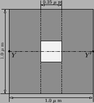
In addition to the three-dimensional plots the resist profiles are compared
along the cut
![]() going through the center of the
contact hole (cf. Figure 8.16).
In Figure 8.27 to Figure 8.29 the
cross sections are shown for the three topographies.
The diameter of the printed contact hole at the substrate surface can
be extracted from the two-dimensional profiles.
The results are summarized in Table 8.2.
going through the center of the
contact hole (cf. Figure 8.16).
In Figure 8.27 to Figure 8.29 the
cross sections are shown for the three topographies.
The diameter of the printed contact hole at the substrate surface can
be extracted from the two-dimensional profiles.
The results are summarized in Table 8.2.
The simulations show the influence of a nonplanar topography on the overall
lithographic performance. In general a reflective material, e.g., a conductor
forming the interconnect between the individual devices, has a strong impact on
the printing quality. For that reason chemical polishing was developed to avoid
the strong nonplanarities occurring during the back-end process
steps [241]. In case of a dielectric material the
effects are less pronounced. The formation of source/drain contacts
is thus less problematic since the nonplanarity is a dielectric like oxide.
Furthermore, the superior performance of advanced
illumination apertures in case of focus errors is demonstrated. Since the
simulated pitch was 1 ![]() m all illumination apertures are capable to resolve
the contact holes. However, in case of coherent illumination the opening
diameter differs considerably between the focus and defocus situation and
process latitude can not be matched. For that reason
advanced illumination apertures are predominantly used in modern semiconductor
lithography.
m all illumination apertures are capable to resolve
the contact holes. However, in case of coherent illumination the opening
diameter differs considerably between the focus and defocus situation and
process latitude can not be matched. For that reason
advanced illumination apertures are predominantly used in modern semiconductor
lithography.