1 Introduction
Comparing the computational capabilities of today’s smartphones to computers from one or two decades ago, the influence of semiconductor technology on our lives is unquestionable. Today, in 2018, a high-end smartphone is built around a
hexa-core or octa-core processor1 running at a clock speed of roughly  GHz and equipped with about
  MB of cache. The processor’s transistors are created using semiconductor manufacturing processes with a
metal pitch2 of about
MB of cache. The processor’s transistors are created using semiconductor manufacturing processes with a
metal pitch2 of about  nm. This results in a total of a few billion transistors on the processor die interconnected with several
kilometers of metal lines. In 2008, similar computing power could be found in a high-end desktop computer with a quad-core processor3 and MB of cache running at a clock speed of around
nm. This results in a total of a few billion transistors on the processor die interconnected with several
kilometers of metal lines. In 2008, similar computing power could be found in a high-end desktop computer with a quad-core processor3 and MB of cache running at a clock speed of around  GHz. This by now outdated processor consisted of about 1 billion transistors with a metal pitch of
  nm. In 1998, a device with similar computing power would have found its place somewhere in the second
half of the famous list of the world’s top 500 supercomputers. Back in the day, in this list, the top-ranked supercomputers consisted of hundreds of interconnected single-core processors4. The metal pitch was around
nm. In 1998, a device with similar computing power would have found its place somewhere in the second
half of the famous list of the world’s top 500 supercomputers. Back in the day, in this list, the top-ranked supercomputers consisted of hundreds of interconnected single-core processors4. The metal pitch was around  nm and processors were clocked around
  MHz.
MHz.
The production of reliable and energy-efficient structures for today’s microprocessors is made possible by the expertise of engineers and researchers at universities and in the semiconductor industry. Most of today’s production processes are conducted in meticulously calibrated reactor setups and are sensitive to variations produced by the preceding processing steps. As a consequence, optimizing a production process or developing a new sequence of processes has become a very expensive endeavor. Thus, computer simulations are more and more used to partly replace expensive and lengthy experimental process runs. In all areas of semiconductor product development, computer simulations have become an integral part and are also key to gain additional insights into the utilized processes.
An important branch of simulation-based electronic design automation is technology computer-aided design (TCAD) which models the fabrication and the operation of semiconductor devices and circuits. The modeling of the fabrication is called Process TCAD and includes simulations of etching, deposition, diffusion, and implantation processing steps. The simulated device structures are forwarded to Device TCAD simulations to determining the electrical characteristics, which in turn are used by Circuit TCAD to simulate the behavior of electronic circuits consisting of multiple interconnected devices.
This work focuses on specific aspects of Process TCAD, where nowadays the decreasing physical dimensions of a single device combined with vertical design layouts demand for three-dimensional simulations. For example, if a three-dimensional geometry cannot be approximated as constant in one dimension, the influence of the surrounding geometry on the etch rates (caused by shadowing of parts of the surface) of a plasma etching process (a key topography-changing process) cannot be considered in a two-dimensional simulation. When keeping the resolution on the surface constant, a three-dimensional simulation increases the computational demands. This is noticeable especially when considering the simulation times for etching processes. The accurate calculation of the etch rates on a highly resolved surface is the primary bottleneck, accounting for the majority of the total runtime of the overall simulation. The models for the etch rates depend on the local surface rates of the etchants. In turn, the computational methods used for surface rate calculation constitute nearly the entire computational load of the etch rate calculation [10]. Therein lies a fundamentally important demand for computationally efficient, high performance numerical methods for the surface rate calculation. This demand is the underlying motivation for this work, which focuses on reducing this common computational bottleneck arising in the three-dimensional simulation of an etching process but also in a deposition process.
The remainder of this section lays the groundwork and is arranged as follows: Section 1.1 provides a brief summary of the typical stages in a microprocessor fabrication process. To motivate this research, Section 1.2 introduces an example application of a plasma etching process and its simulation. Finally, the research goals are formulated in Section 1.3 and an outline for the rest of this work is provided in Section 1.4.
1 Apple A11 Bionic (hexa-core), Samsung Exynos 9 Series (octa-core)
2 The minimum lateral distance between 2 transistor contacts.
3 Intel i7 CPU 940 (quad-core)
4 Sun UltraSPARC I/II, IBM POWER2 SC
1.1 Semiconductor Processing
As this work investigates problems within the general setting of Process TCAD, here, typical processing steps are discussed in an abstract manner to provide the context for the discussed topics. The following items provide a brief overview of the processing stages during the production of a microprocessor:
-
(a) The surface of the silicon wafer is prepared for the first processing steps, e.g., cleaned and polished.
-
(b) A specific sequence of processing steps is performed to create the transistors at the desired positions. Depending on the technology of the chip generation, the processing sequence is different. Common processing steps include, lithography, etching, deposition, oxidation, implantation, diffusion, and planarization. A majority of the etching and deposition processing steps are conducted in a vacuum reactor; the goal is to expose the full wafer surface to a controlled environment to maximize the yield, i.e., the portion of properly functioning devices. The gas phase in the reactor is composed out of one or more process gases; the gas composition is chosen to induce the desired surface reaction on the exposed materials stack on the wafer.
-
(c) By subsequent processing steps, vertical metal contacts to the terminals of the devices (e.g., transistors) are created and the devices are sealed with a dielectric.
-
(d) The following processing steps create the conducting connections between, for example, the transistor terminals according to the circuit design. To achieve complex connection networks, multiple layers of metal lines, vertically connected through vias, are necessary. The first metal layers start with a pitch size similar to the transistor pitch. The subsequent metal layers have incrementally increasing dimensions, where the dimensions of the outermost metal layer are suitable to connect the processor to the periphery.
-
(e) The separation of the wafer into single semiconductor chips is the last processing step on the full wafer; it is typically followed by packaging each individual chip into a form suitable for the final application target.
Items (b) to (c) are typically referred to as front-end-of-line; (d) is called back-end-of-line. Both together represent the front-end of the production, while step (e) is referred to as back-end of production.
1.2 Motivational Example: Plasma Etching Simulation for Copper Interconnects
Etching is a fundamental processing step. To further outline the challenges and approaches associated with it, an exemplaric etching simulation scenario is introduced and discussed in order to motivate the research presented in this work.
First, a sequence of processing steps, used to fabricate a copper metal layer, is introduced. Then, a brief characterization of a plasma etching process in general is provided by relating it to one of the processing steps, namely the plasma etching of a dielectric layer. It follows a discussion on the demarcation between reactor-scale and feature-scale simulations. Then, an etching simulation of the aforementioned dielectric layer is presented. The commonly involved models and typical choices for computational tasks are briefly discussed and the runtime consumed by these tasks is put in relation.
Copper Interconnect Fabrication
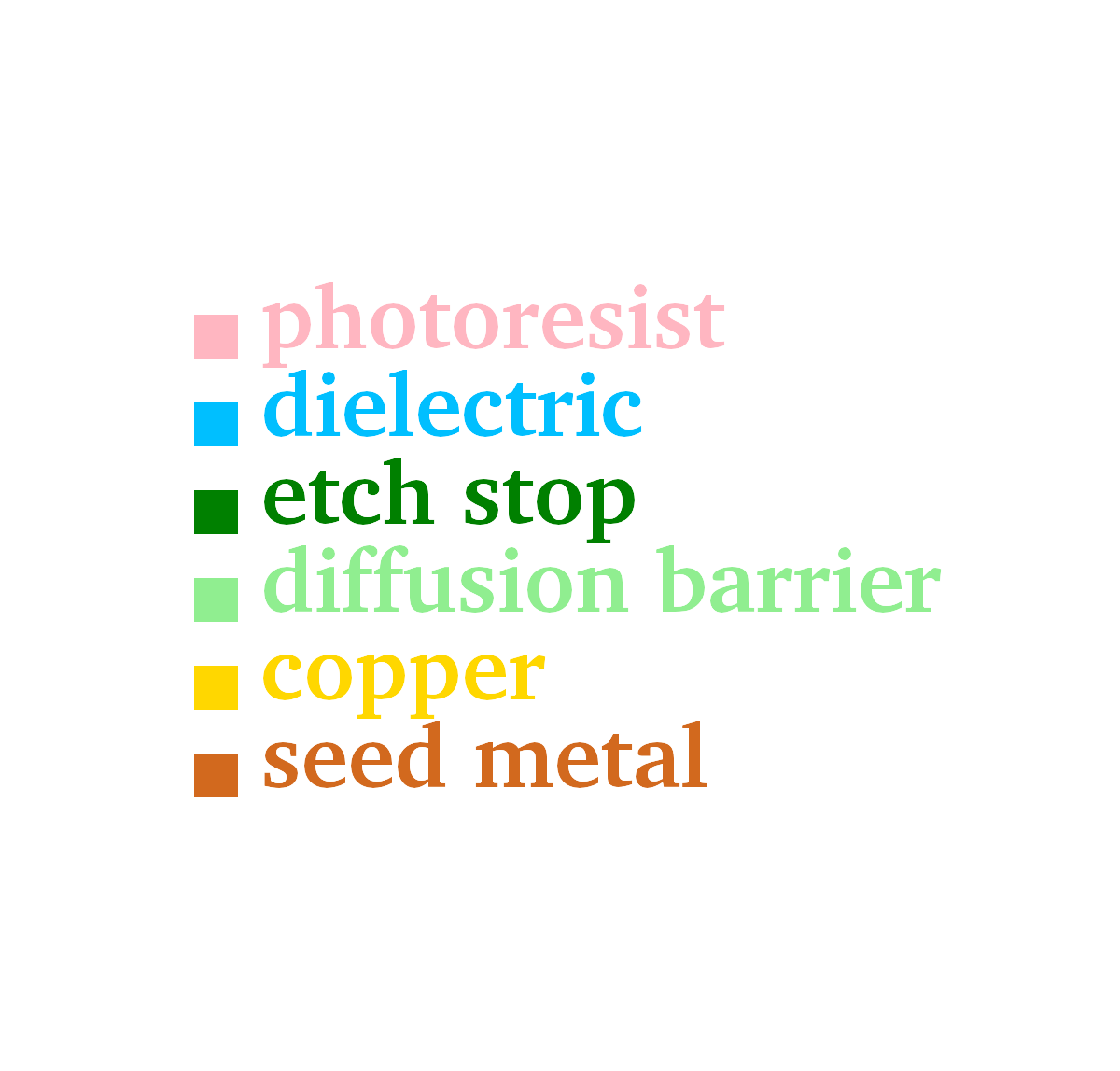
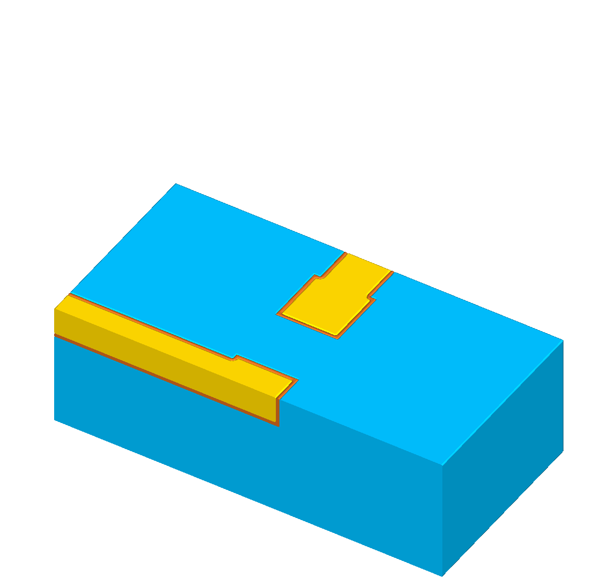
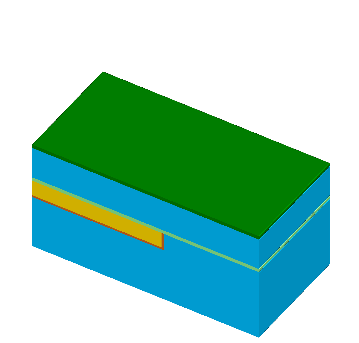
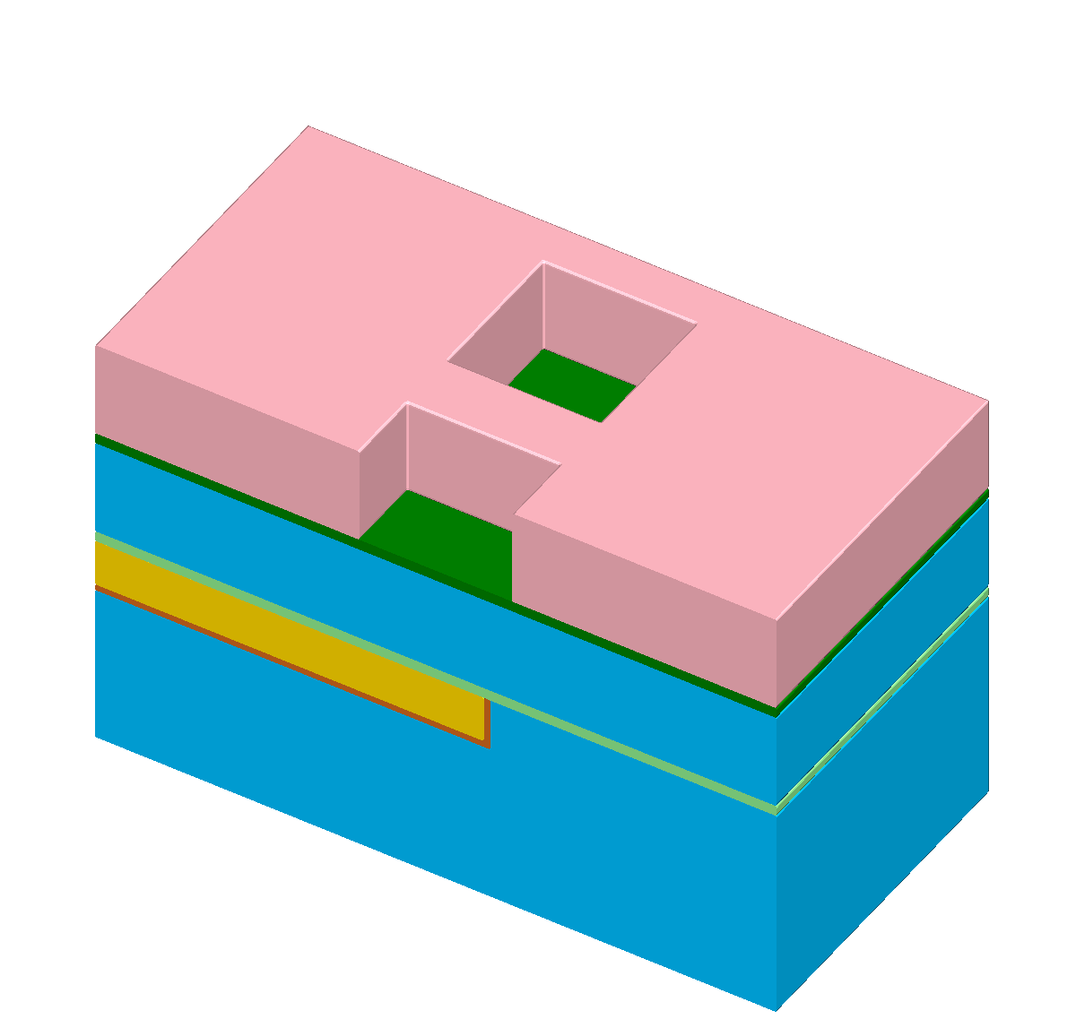
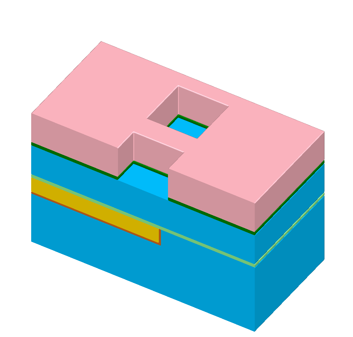
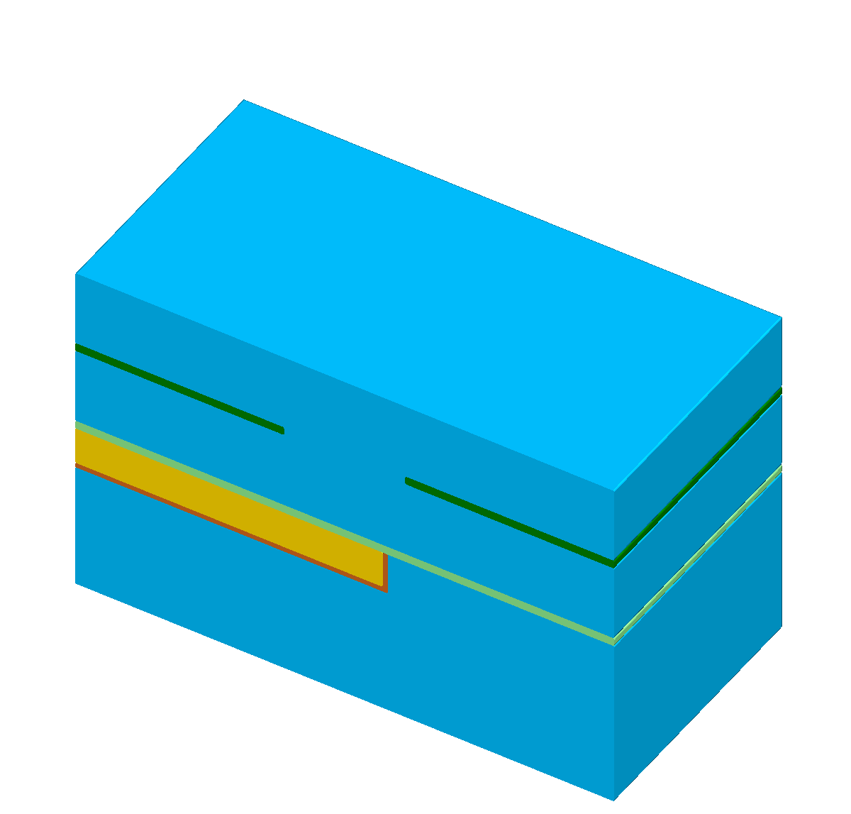
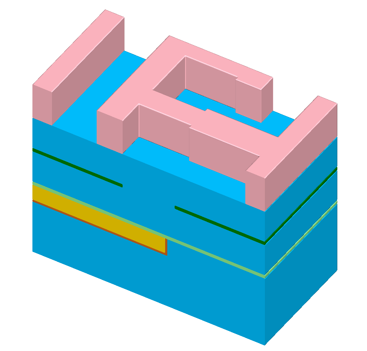
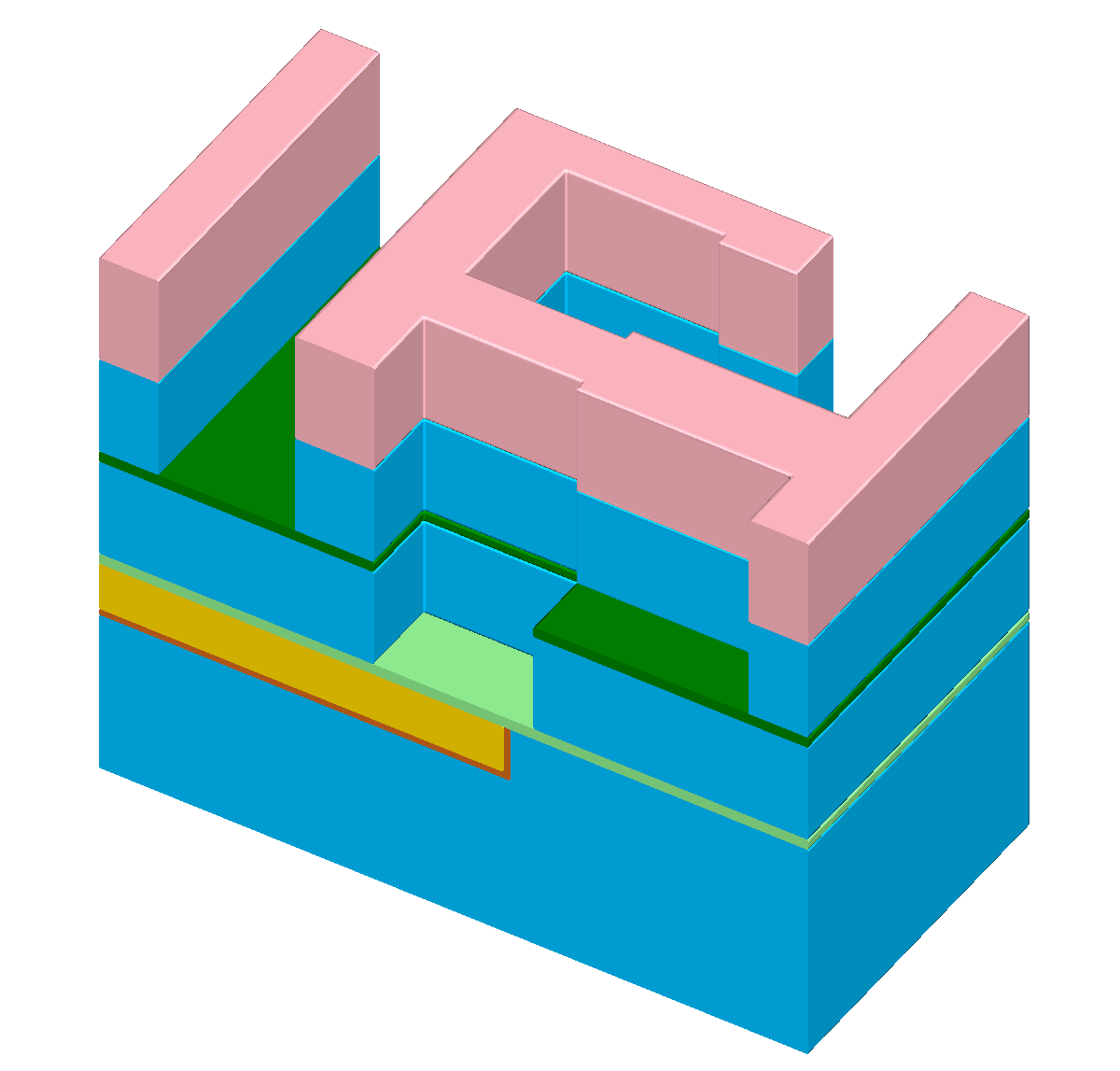
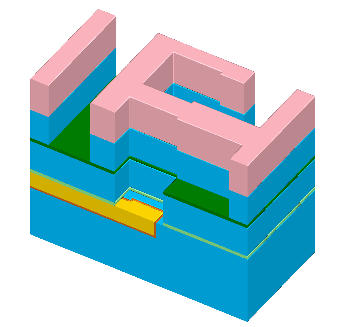
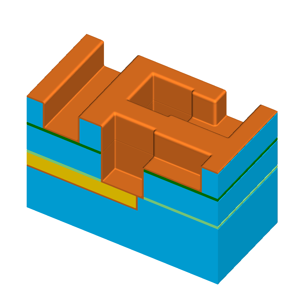
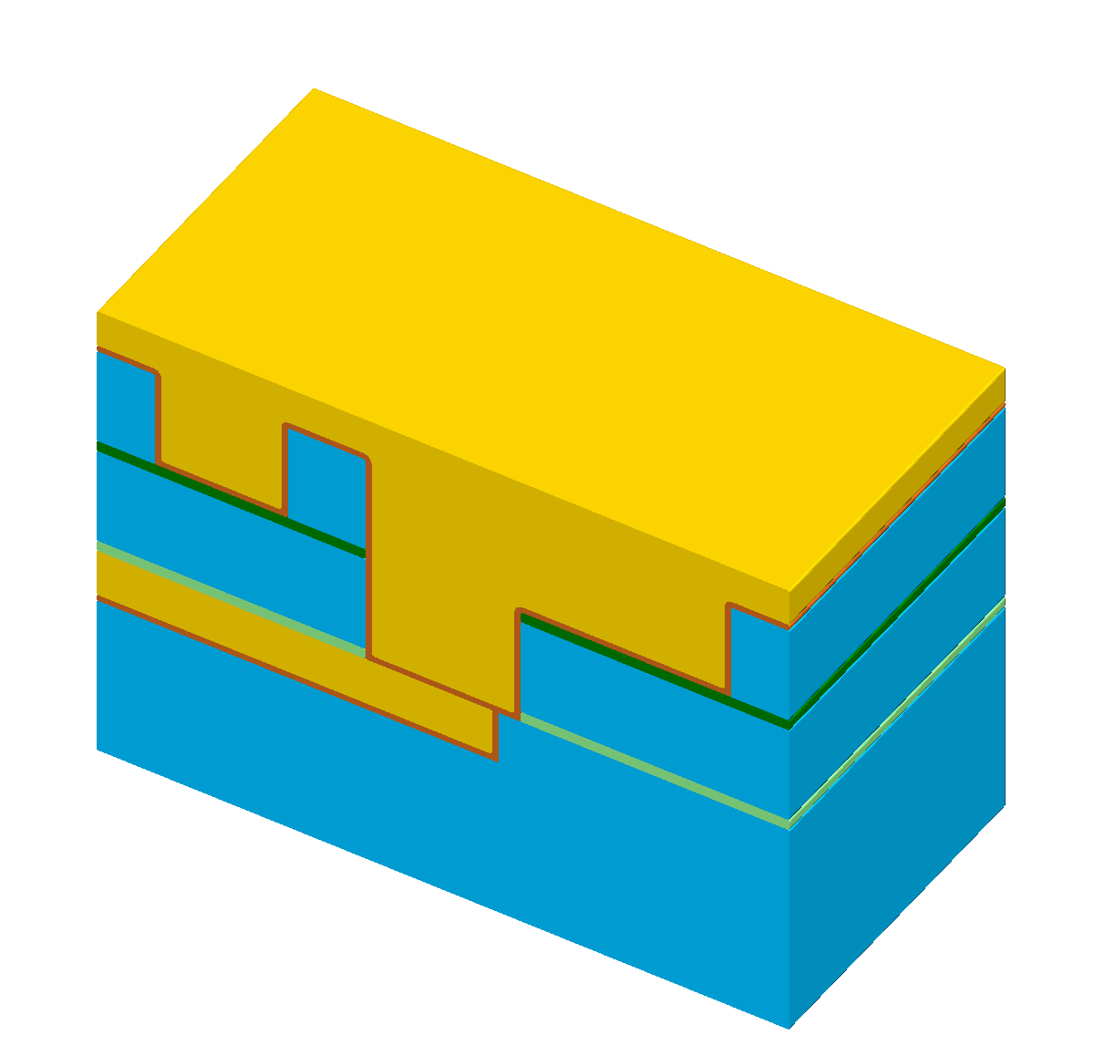
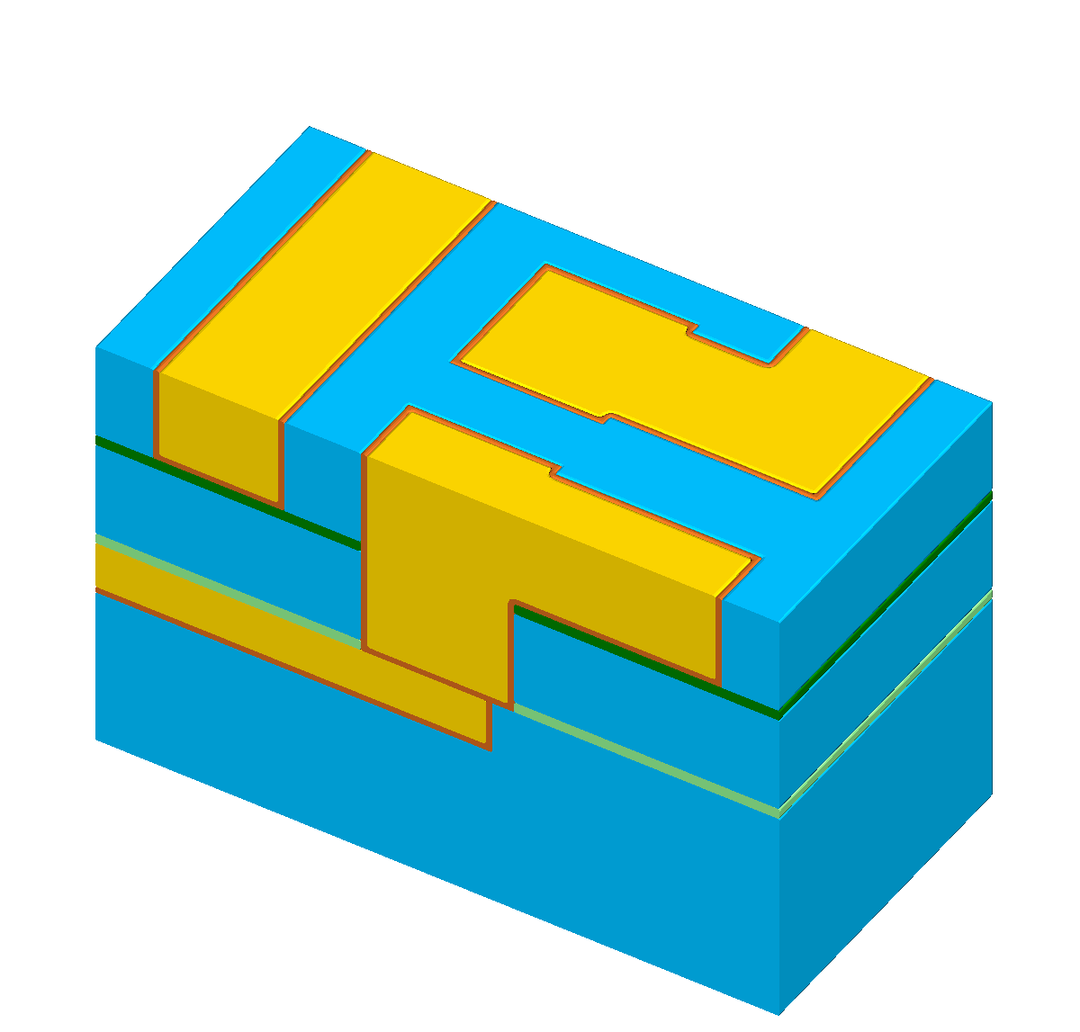
Figure 1.1: The “self-aligned dual-damascene process” is used to create a copper metal layer. Figures (b) to (l) illus- trate all processing steps to create a metalization layer on top of an existing metalization layer (the square domain is clipped along one axis for better visibility). First row (b) to (c): Initial patterned planar conductor and deposition of three layers: A diffusion barrier, a dielectric material, and an etch stop material. Second row (d) to (f): Patterning of the etch stop layer (at the position of the vias) including the deposition of the second dielectric layer. Third row (g) to (i): Patterning of the dielectric layers (vias and lines) including opening of the diffusion barrier layer around the position of the via. Last row (j) to (l): Copper metalization including the deposition of a metal seed layer and chemical-mechanical planarization after the copper deposition.
There are various process sequences to fabricate a metal layer above an existing metal layer [59]. All have in common that vertical conducting connections (vias) as well as horizontal connections (lines) have to be created and bonded together. Depending on the metal used for the connections, the required process sequence can be quite different. Here, we introduce a basic process sequence referred to as “self-aligned dual-damascene process” [59][74]. It is used to process a copper metal layer including vias and lines [73]. The processing steps are visualized in Figure 1.1 for a generic connection layout with three vias; the following describes each step in more detail:
-
(a) Legend of the different materials involved in the following steps.
-
(b) Initial surface of the wafer: The lines of the lower metal layer are visible; the position for the vias to the next metal layer are noticeable as the diameter is widened slightly. The copper region is surrounded by a metal seed layer.
-
(c) Three layers are deposited on the planar surface: A thin barrier to prevent the copper region from diffusing into the dielectric layer, a thick dielectric layer to embed the vias, and a thin etch stop layer on top of the dielectric layer.
-
(d) A photoresist is patterned on top of the dielectric layer with the positions of the vias.
-
(e) The pattern of the photoresist is transferred to the etch stop layer.
-
(f) After the photoresist is removed, a second dielectric layer is deposited to embed the metal lines. The two dielectric layers are now directly connected at the desired positions of the vias.
-
(g) Again, a photoresist is patterned on top of the dielectric layer, now patterned with the vias and lines.
-
(h) The pattern of the vias and lines is transferred to the dielectric layers using a single plasma etching process. The images show the result of perfect vertically selective etching and without any etching of the etch stop layer and diffusion barrier.
-
(i) The exposed area of the diffusion barrier is removed and the underlying copper contact is now open.
-
(j) A thin layer of seed metal is deposited on the whole surface; it serves as a seed for the crystallization and prevents the copper from diffusing into the dielectric layer.
-
(k) The cavities for the vias and lines are overfilled with copper using a deposition process.
-
(l) In a chemical-mechanical-planarization process, the copper above the dielectric layer is removed and a planar wafer surface is obtained; ready to start with the next metalization layer.
Plasma Etching Process
The etching of the dielectric material during the metal layer processing (Figure 1.1h) is in practice realized using a plasma etching process which exposes the wafer surface to a reactive gas phase (plasma) in a vacuum reactor. The gas phase in the reactor is controlled with a gas inlet and a gas outlet leading to a permanent gas stream. The volatile reaction products are carried away with the gas stream, while other reaction products may stick to the wafer surface or re-deposit on another location. Usually, the etching process is conducted for a predefined time span. A wide variety of plasma etching configurations to achieve various processing goals exist. The configurations differ with regard to the pressure and temperature inside the reactor, the composition of the gas phase, how the plasma is created, and if (or how) the ions in the plasma are accelerated towards the wafer surface.
Simulation Types
Etching process simulations can be partitioned into two major types [22]:
- Reactor-Scale.
-
The simulation domain is the full reactor chamber or an important part of it [80], which enables, for example, that uniform properties of the angular and energetic particle distribution in the gas phase over the full surface of the wafer can be an optimization target. Geometric details of the topography on the wafer surface are not modeled explicitly.
- Feature-Scale.
-
The simulation domain is a region of the wafer surface. A common reason for a feature-scale simulation of an etching process is to predict the topographical change of the material stack in the region of interest.
Due to this work’s focus on three-dimensional feature-scale simulations, the following provides more details for this type of simulation.
Feature-Scale Etching Simulation
The simulation domain of a feature-scale simulation is usually a rectangular region of the wafer surface containing all geometry details of the stacked materials — forming a device — generated in the preceding processing steps. The lateral boundaries of the simulation domain are usually modeled using reflective or periodic boundary conditions. At the top, towards the reactor chamber, the simulation domain is delimited by a “source plane”. By defining angular and energetic distributions of the involved process gas species on the source plane, reactor-scale and feature-scale simulations are decoupled. Figure 1.2 shows an example of a feature-scale simulation domain using the same material stack and geometry introduced in Figure 1.1.
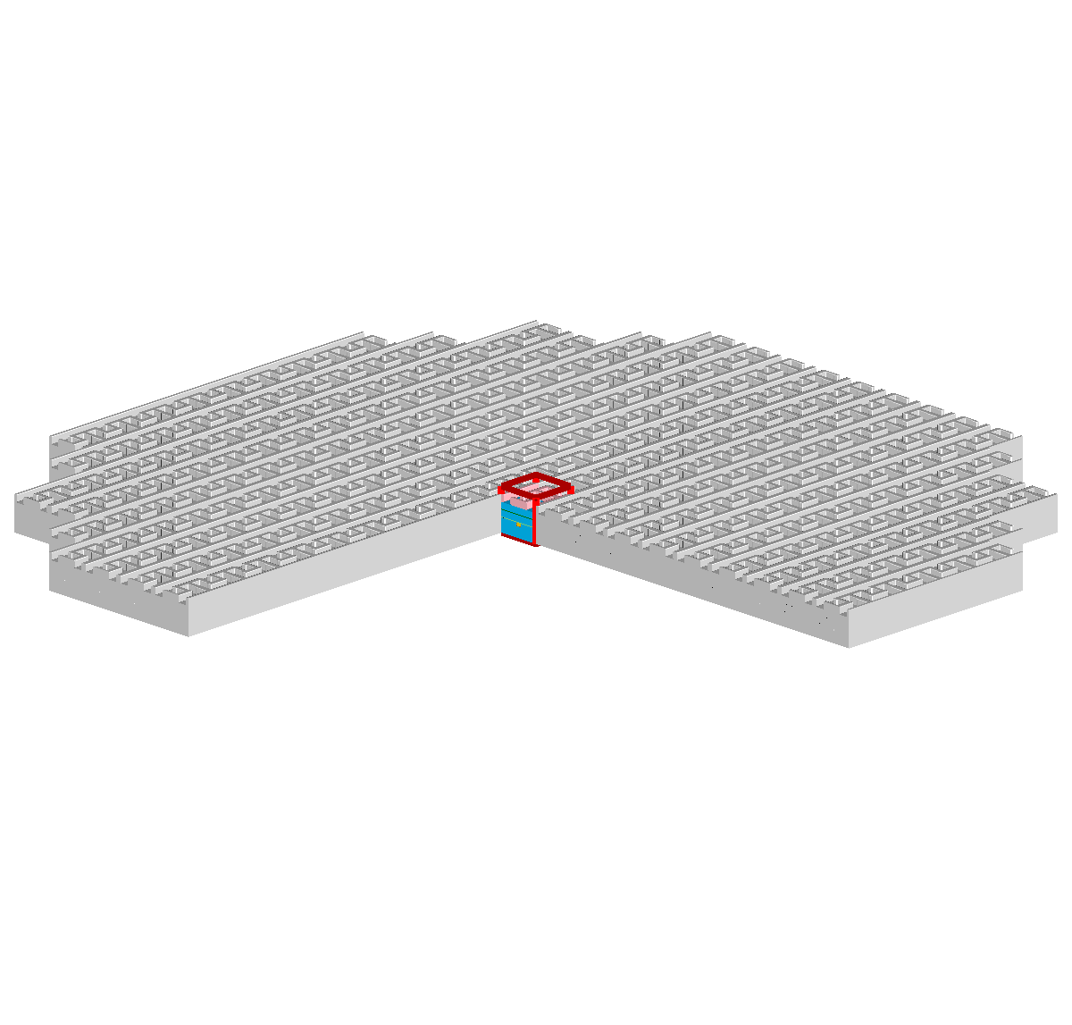
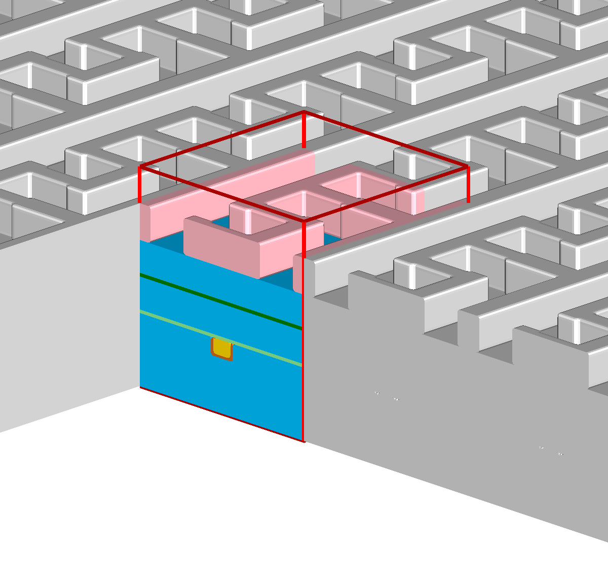
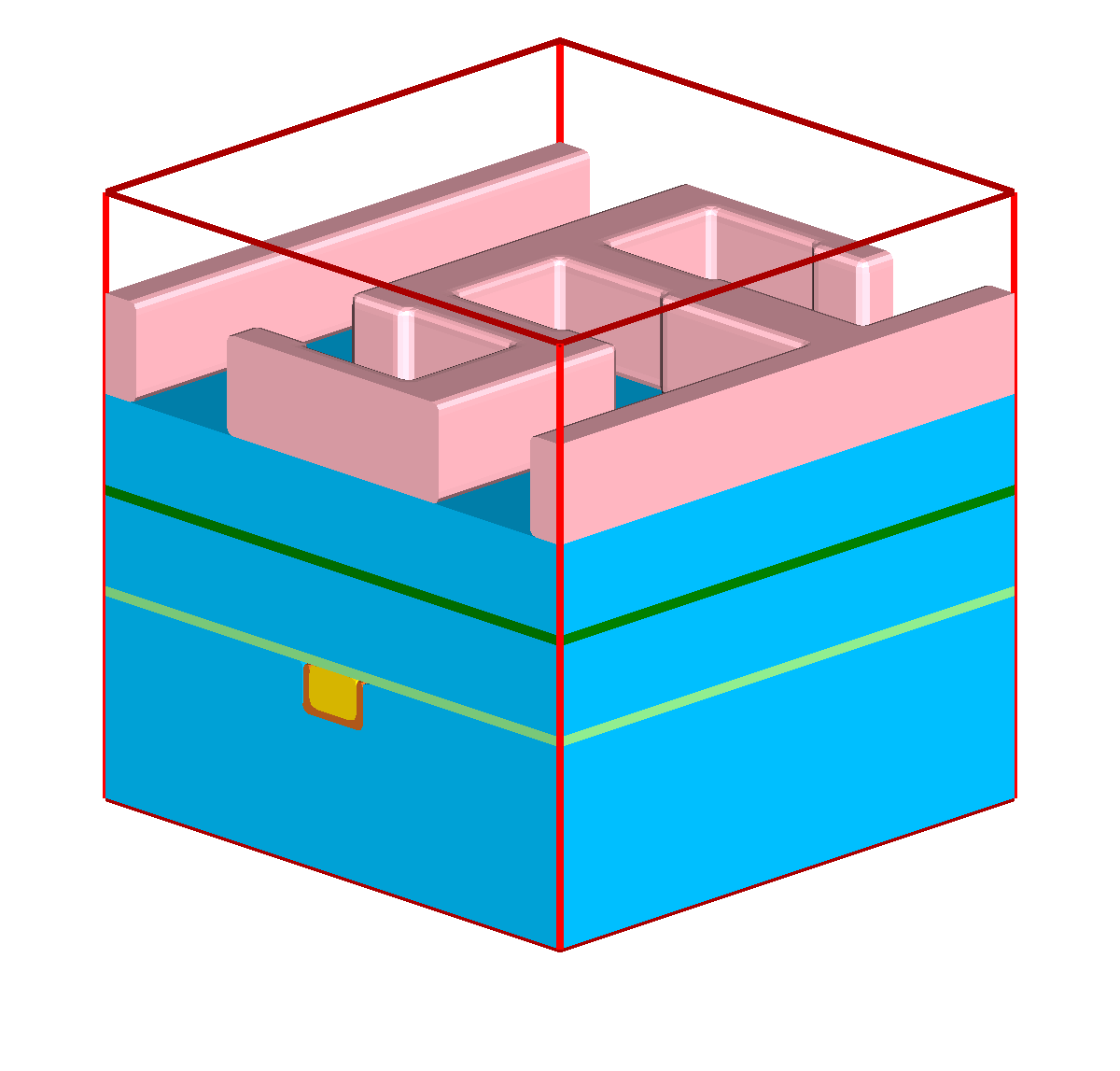
In Figure 1.1h, the result of the etching process is only shown schematically, assuming perfect vertically selective etching and no etching of the other exposed materials. In contrast, Figure 1.3 illustrates the resulting topography when the etching process is simulated in a three-dimensional feature-scale simulation. Without any knowledge about the simulation models in use, it is apparent that all exposed materials are influenced during the etching process. How the topography changes during the etching process is defined by the model for the local etch rates, or more generally, the surface velocities. In advanced models the surface velocity depends on the particle transport of the involved gases inside the feature-scale simulation domain. These advanced models are important for three-dimensional etching and deposition simulations in general and inevitable for high aspect ratio geometries (cf. Chapter 7), where the results are sensitive to the accuracy of the solution to the particle transport.
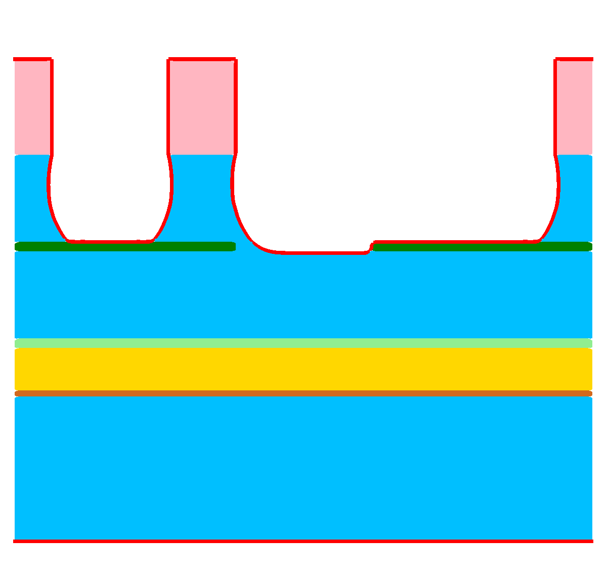

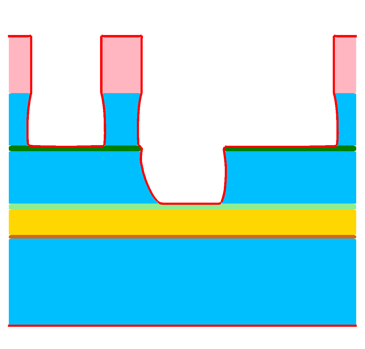

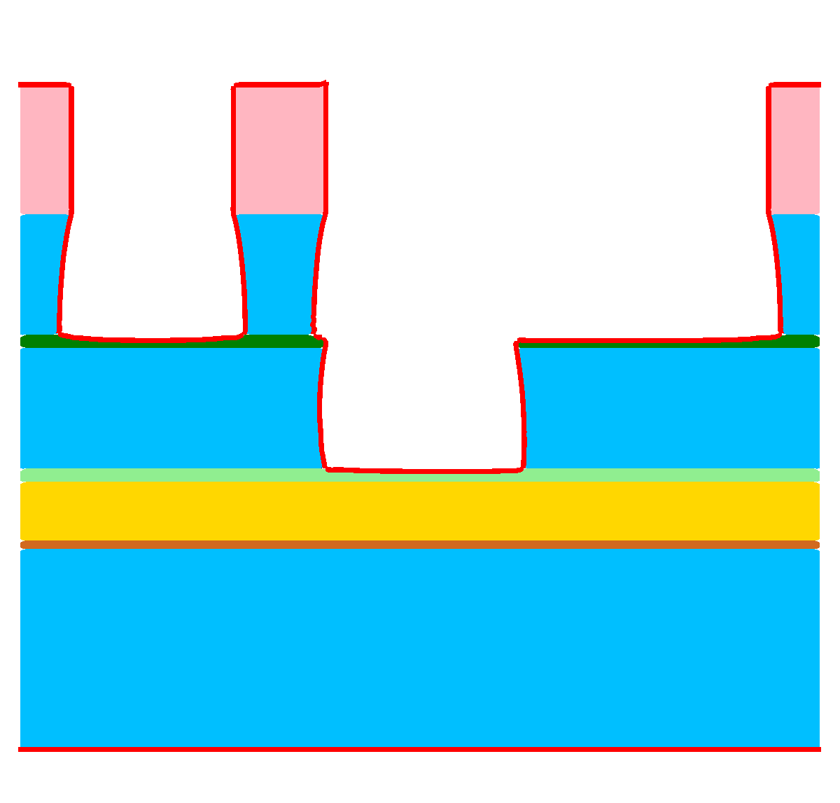
Figure 1.3: Results of a feature-scale etching simulation of the dielectric layer in a “self-aligned dual-damascene process” (cf. Figure 1.1h). (a)
Initial domain. (b)-(d) Clipped view of the three-dimensional domain for ![\( T=[0.5,1.0,1.5] \)](lateximages/16C917D73083166CEFE056353577D5A0.svg) . The top surface, which is exposed to the process gases, is visualized
as red line.
. The top surface, which is exposed to the process gases, is visualized
as red line.

Figure 1.4: Runtime of the main computational tasks (logarithmic scale) for all time steps ( to
to  ) (cf. Figure 1.3).
Surface Velocity
The particle transport through the gas phase to the surface yields a surface rate distribution for each particle type on the exposed surface. Depending on the particle type, the rate is included in the surface velocity model as a flux rate or
sputter rate for neutral particles and accelerated particles (ions), respectively. In simple models, a linear dependence on the surface rates is assumed for the surface velocity. The normal surface velocity  at position
  on the surface can the be written as

where  is the number of simulated particle types,
  is the surface rate of particle type
  at position , and
  is a factor depending only on the material
  at .
at .
Particle Transport
To obtain the surface rate distributions  on the surface, the transport of the particles from the source plane
to the surface must be computed. Due to the low pressures in the reactor chambers and the small geometric extensions of the feature-scale region, particle-particle collisions are typically neglected as the mean free path of a particle is much larger
than the domain extensions [22]. This justifies the assumption of ballistic transport of particles and the use of line-of-sight methods, if electromagnetic forces on charged particles are neglected.
on the surface, the transport of the particles from the source plane
to the surface must be computed. Due to the low pressures in the reactor chambers and the small geometric extensions of the feature-scale region, particle-particle collisions are typically neglected as the mean free path of a particle is much larger
than the domain extensions [22]. This justifies the assumption of ballistic transport of particles and the use of line-of-sight methods, if electromagnetic forces on charged particles are neglected.
Depending on the properties of particle sources, material properties, and feature geometry, the incorporation of the re-emission of particles from the surface in the transport model can be very important. For example, in the etching simulation of a high aspect ratio trench, the vertical surface rate distribution of particles is strongly influenced by the re-emission properties of the sidewalls (cf. Section 7.3).
The numerical methods used to model the particle transport can be divided into three main groups:
-
(a) In the “straightforward approach”, the surface, as well as the source plane, is discretized into
 elements (e.g., using triangles). Furthermore, also the angular and energetic
flux distribution is discretized by an appropriate set of
elements (e.g., using triangles). Furthermore, also the angular and energetic
flux distribution is discretized by an appropriate set of  basis functions (e.g., subdivision of the solid angle and a binning scheme for
energies). From this discretization, a linear system of equations with
basis functions (e.g., subdivision of the solid angle and a binning scheme for
energies). From this discretization, a linear system of equations with  unknowns and
  non-zero entries is assembled. Constructing the system matrix
requires visibility information between all elements.
non-zero entries is assembled. Constructing the system matrix
requires visibility information between all elements. -
(b) In the bottom-up iterative scheme, the surface is discretized and the direct flux for each surface element is calculated by numerical integration over the solid angle under which the source plane is visible. For each surface element, an averaged representation of the incoming particles is maintained. A number of iterations is then performed, where the flux rates are updated by numerical integration over the solid angle under which the surface is visible. The number of iterations is equal to the number of considered re-emissions.
-
(c) In the top-down approach, the surface is discretized and particles are traced from random locations on the source plane according to the angular and energetic distribution of the particle sources. At the first intersection with the surface, a contribution to the local surface rate is calculated and a new particle is re-emitted according to the local surface re-emission properties. After a fixed number of re-emissions or a threshold condition for the energy of the particle the tracing is terminated.
All three approaches have in common that a large number of visibility/intersection tests are involved, either providing the information if two points in the domain are mutually visible (not obscured) or which is the first element intersecting a path starting from an element in a certain direction.
The particle transport calculation has to be repeated in each time step of a simulation due to the changed topography of the surface. When using any of the numerical methods listed above in a three-dimensional etching simulation, it constitutes the major part of the computational load in each time step.
Surface Advection
The advection of the exposed surfaces is preferentially realized by the utilization of the level-set method (cf. Section 2.1). In contrast to
cell-based or mesh-based methods, it provides a robust framework to deal with topological changes of the surface, for example, when a surface splits in two parts or merges with itself. The level-set equation (1.2) relates the temporal change of a scalar level-set function  to the norm of the gradient of using a scalar velocity field
  as a prefactor. The velocity field
  is not only defined on the surface, but in the whole domain. It is
constructed via an appropriate extension of the surface velocities ; a simple construction scheme is to use the value at the closest point on the
surface.
is not only defined on the surface, but in the whole domain. It is
constructed via an appropriate extension of the surface velocities ; a simple construction scheme is to use the value at the closest point on the
surface.

Common practice is to initialize so that the surface in question is represented implicitly by the zero-level-set
of . The evolution of the surface over time is obtained by solving (1.2). The spatial discretization of  is usually accomplished using suitable higher-order finite-difference
schemes on a Cartesian grid [14]. A simple choice for the temporal discretization is the explicit Euler method. To obtain a stable scheme, a maximum time step of
is usually accomplished using suitable higher-order finite-difference
schemes on a Cartesian grid [14]. A simple choice for the temporal discretization is the explicit Euler method. To obtain a stable scheme, a maximum time step of

is necessary, where  is the spatial grid spacing,
  is the maximum value in the velocity field, and
 ![\( \alpha _{CFL} \in \ ]0,1] \)](lateximages/8AF8B2FE10C9608A9ED9D8AE10A0AEBB.svg) is a positive constant depending on the discretization
(cf. Section 2.3). As a consequence, for a given physical simulation time, the number of necessary time steps grows linear with the resolution of
the surface.
is a positive constant depending on the discretization
(cf. Section 2.3). As a consequence, for a given physical simulation time, the number of necessary time steps grows linear with the resolution of
the surface.
Computational Demands
Assuming the level-set method is used for surface advection, the common computational tasks in one time step of a simulation are
-
(a) the preparation of a suitable surface representation for the surface rate calculations,
-
(b) the calculation of the surface rate distributions on the surface,
-
(c) the evaluation of the surface velocity models using the surface rate distributions, and
-
(d) the advection of the level-set function according to the computed surface velocity field (e.g., solving (1.2)).
Figure 1.4 depicts the runtime for each of these tasks based on an exemplary etching simulation of the dielectric layer shown in Figure 1.3. The simulation is performed on a 16-core workstation (WS2, cf. Section 3.4) and the surface rate calculation is parallelized
(OpenMP, 32 threads) as well as the surface advection. The horizontal resolution of the domain is  grid cells. The surface velocity is modeled using a vertically focused
source of a single particle species according to
grid cells. The surface velocity is modeled using a vertically focused
source of a single particle species according to

In the particle transport model only the direct flux rate is considered; a bottom-up approach with  sampling directions to integrate the arriving particle distribution at each surface element is used. The
calculation of the surface rates consumes the major part of the overall runtime of the simulation.
sampling directions to integrate the arriving particle distribution at each surface element is used. The
calculation of the surface rates consumes the major part of the overall runtime of the simulation.
1.3 Research Goals
The goal of this work is to provide techniques to reduce the calculation time of particle transport models – constituting the major computational bottleneck – in three-dimensional feature-scale process simulations. In particular, the focus is on etching and deposition processes. Figure 1.4 shows that even for low surface resolutions and simple models for the particle transport, e.g., only considering the direct flux rate and ignoring contributions from re-emissions, the surface rate calculation by far takes up the majority of the overall runtime of the simulation: A perceptible speedup of the underlying numerical methods of the surface rate calculation would therefore equate to a nearly identical speedup for the overall runtime; this holds for a wide range of etching as well as deposition simulations. Such a runtime reduction is highly desirable as it paves the way for high surface resolutions and the option to integrate advanced models capturing effects neglected before because of unfeasible simulation runtimes.
Another important goal of this work is to develop numerically robust methods for arbitrary geometries, which have a clear interface and can be straightforwardly integrated into existing simulation tools.
The research presented in this work was conducted within the scope of the Christian Doppler Laboratory for High Performance Technology Computer-Aided Design (TCAD). The Christian Doppler Association funds cooperations between companies and research institutions pursuing application-orientated basic research. In this case, the cooperation was established between the Institute for Microelectronics at the TU Wien and Silvaco Inc., a company developing and providing electronic device automation and TCAD software tools.
1.4 Outline of the Thesis
Chapter 2 provides an overview of currently available software frameworks for feature-scale process simulations and introduces commonly used numerical methods for the particle transport, which are a focus for this work. The level-set method (including its common discretization schemes) is introduced in more detail as it is used as foundation for the surface advection in many frameworks.
Chapter 3 introduces the developed simulation platform which is used in all subsequent chapters to implement, validate, and test the accuracy and performance of new numerical approaches for the flux rate calculation.
Chapter 4 presents an approach to accelerate the direct flux calculations in three-dimensional process simulations: Using a subdivided icosahedron to define the search directions, it is shown that the surface rate calculation can be accelerated by a factor of at least two when adaptively refining the search directions only near the aperture boundary. If the refinement is initialized on a level appropriate to the expected topography, the accuracy of the resulting surface rates is not reduced.
Chapter 5 presents an approach to perform the visibility calculations for the surface rate calculation on a temporarily generated explicit surface mesh utilizing modern hardware-tailored single-precision ray tracing frameworks. When compared to ray tracing directly on the level-set data structure, a speedup of at least a factor of 3 is attested.
Chapter 6 presents an approach to evaluate the surface rates only on a sparse set of points on the surface to reduce the computational effort. This sparse set of points is generated according to application-specific requirements using an iterative partitioning scheme. The resulting sparse surface rates are “diffused” in the neighborhood to approximate a linear interpolation on the whole surface. The obtained speedup factors range from 2 to 8 and the produced deviations of the surface position are below 3 grid cells for all tested cases.
Chapter 7 introduces a radiosity-based method to approximate the flux rates of neutral particles in very high aspect ratio holes and trenches. It is based on a one-dimensional approximation of the three-dimensional surface and is eligible if simulation runtime is critical and the geometry can be approximated with a convex rotationally symmetric hole or convex symmetric trenches.
Chapter 8 demonstrates the overall obtained speedup when applying the approaches presented in Chapters 4 to 6 in conjunction.
Finally, Chapter 9 concludes with a brief overall summary and presents ideas for future work.