« PreviousUpNext »Contents
Previous: 1.4 Three-Dimensional Integration Top: 1 Introduction Next: 1.6 Failure Mechanisms in Interconnects
1.5 Open TSV Structure
A recent TSV design is realized by filled copper TSVs and has the advantage of a low contact resistance [81]. However, the price of a high mechanical stress due to the mismatch of the thermal expansion coefficient of the TSV
materials and the substrate has to be paid [122]. Furthermore, the depth of the TSV structure is limited to approximately  determined by the limitation of the
aspect ratio of the etching process and the limited thicknesses of copper deposited by electroplating. Therefore, the open TSV structure was introduced, where the filling of the vertical cylindrical structure is replaced by a
metallization layer plated on the cylindrical wall leaving it hollow, as depicted in Figure 1.4. The fabrication of the open TSV structure is carried out after the front-end and back-end metallizations are performed in a regular CMOS
process. In the following sections the steps for the open TSV fabrication are presented for a sensor chip which is wafer bonded on a CMOS wafer [83].
determined by the limitation of the
aspect ratio of the etching process and the limited thicknesses of copper deposited by electroplating. Therefore, the open TSV structure was introduced, where the filling of the vertical cylindrical structure is replaced by a
metallization layer plated on the cylindrical wall leaving it hollow, as depicted in Figure 1.4. The fabrication of the open TSV structure is carried out after the front-end and back-end metallizations are performed in a regular CMOS
process. In the following sections the steps for the open TSV fabrication are presented for a sensor chip which is wafer bonded on a CMOS wafer [83].
1.5.1 Wafer Bonding
After the final via layer has been processed the top wafer gets thinned to a thickness of  and fine polished at the backside
to a roughness of
and fine polished at the backside
to a roughness of  to obtain
a suitable surface quality for the wafer bonding. The bond interface of the bottom wafer is prepared by oxide deposition employing a plasma-enhanced chemical vapor deposition (PECVD) technique [45], a densification step, and a
chemical-mechanical polishing step which results in a low surface roughness without any nano-topology larger than
to obtain
a suitable surface quality for the wafer bonding. The bond interface of the bottom wafer is prepared by oxide deposition employing a plasma-enhanced chemical vapor deposition (PECVD) technique [45], a densification step, and a
chemical-mechanical polishing step which results in a low surface roughness without any nano-topology larger than  . After removing organic contamination and small particles
with a cleaning step, the bond surfaces are activated by a nitrogen plasma, followed by a further cleaning step, and aligning of the bottom and the top wafers to each other. By bringing them into contact a bond wave is started [108].
The smoothness of the surfaces has to be guaranteed as otherwise the bond wave propagation is disrupted leading to unbonded regions. This can result, beside others, in a chip off, which is the unwanted unbonding of dies, or
increased resistance. The bond wave step is followed by an annealing step resulting in a bond strength of
. After removing organic contamination and small particles
with a cleaning step, the bond surfaces are activated by a nitrogen plasma, followed by a further cleaning step, and aligning of the bottom and the top wafers to each other. By bringing them into contact a bond wave is started [108].
The smoothness of the surfaces has to be guaranteed as otherwise the bond wave propagation is disrupted leading to unbonded regions. This can result, beside others, in a chip off, which is the unwanted unbonding of dies, or
increased resistance. The bond wave step is followed by an annealing step resulting in a bond strength of  . These steps are
followed by a deep reactive ion etch (DRIE) process, the so called Bosch [40] process, described in the following.
. These steps are
followed by a deep reactive ion etch (DRIE) process, the so called Bosch [40] process, described in the following.
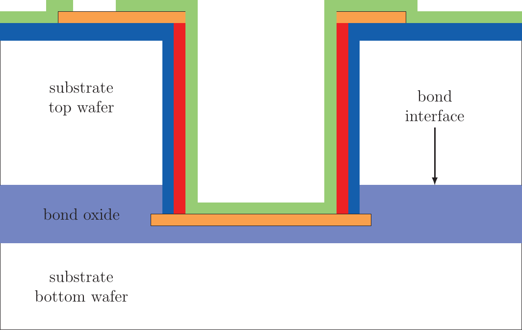
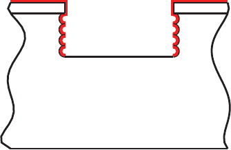
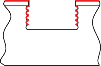
Figure 1.4.: Schematic of the TSV [83]. The orange regions are aluminium, the red are tungsten, the dark blue are the galvanic isolation layer from the metal to the silicon bulk, and the green are the passivation layers. For bonding the bottom wafer is prepared with a silicon oxide (in light blue) and the top wafer is planarized silicon.
1.5.2 The Bosch Etching Process
The Bosch process [23, 31] is a sequence of alternating dry plasma etching and polymer deposition cycles, each lasting only in the range of seconds. The main advantage is the highly anisotropic etching which provides the ability of high aspect ratios between TSV heights and TSV diameters as well as ensuring high mask selectivity and almost vertical sidewalls [85].
The process is carried out by the following steps. First of all the silicon wafer must be covered with a photoresist. This photoresist is exposed to a patterned intensive light causing chemical reactions which allow the removal of the
photoresist at the exposed positions by the developer [123]. The remaining parts of the photoresist form the mask which is necessary to prevent the covered material from being etched. This mask producing process stage is followed
by the actual series of the alternating plasma etching and polymer deposition cycles. For the etching process sulfur hexafluoride  together with a carrier gas (mostly
argon) is injected into the reactor containing the wafer. By the generation of a high energetic plasma the is transformed into a highly reactive
gas realizing an isotropic, chemical etching reaction. This etching is combined with a physical etching realized by the sputtering of ions adding an anisotropy. This step is followed by polymerization, where the before created structure
is passivated by coating it with a polymer layer. For this step fluorocarbons such as
together with a carrier gas (mostly
argon) is injected into the reactor containing the wafer. By the generation of a high energetic plasma the is transformed into a highly reactive
gas realizing an isotropic, chemical etching reaction. This etching is combined with a physical etching realized by the sputtering of ions adding an anisotropy. This step is followed by polymerization, where the before created structure
is passivated by coating it with a polymer layer. For this step fluorocarbons such as  and a carrier gas is
led into the reactor. This mixture is activated and forms a polymer passivation layer on the mask as well as on the sidewalls and on the bottom of the etched trench. The polymerization step is followed by a further etching cycle. In
this cycle due to the anisotropy of the etching process the passivation layer in the bottom of the trench is first etched through. Therefore at the bottom the etching of the silicon starts again, whereas the sidewalls are still protected by
the passivation layer, attaining the anisotropy of the overall alternating process. The trench narrows as the depth increases and the polymer is continuously recoating the structure. These two cycles are repeated, until the requested
TSV depth is achieved.
and a carrier gas is
led into the reactor. This mixture is activated and forms a polymer passivation layer on the mask as well as on the sidewalls and on the bottom of the etched trench. The polymerization step is followed by a further etching cycle. In
this cycle due to the anisotropy of the etching process the passivation layer in the bottom of the trench is first etched through. Therefore at the bottom the etching of the silicon starts again, whereas the sidewalls are still protected by
the passivation layer, attaining the anisotropy of the overall alternating process. The trench narrows as the depth increases and the polymer is continuously recoating the structure. These two cycles are repeated, until the requested
TSV depth is achieved.
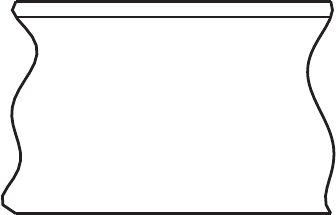
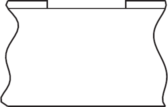
(a) Wafer coated with photoresist away (b) Photoresist washed by the developer.
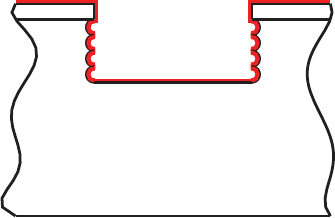
(c) Passivation by coating with a polymer. (d) Etching of the polymer till the bottom silicon is free.
(e) Etching of another well. This step is followed by the passivation step (c).
1.5.3 Isolation and Metallization of the Open TSV
After the sequentially repeated etching and passivation processes have reached the metallization layer of the bottom wafer isolation, lining and passivation processes have to be carried out. For the isolation of the conductive TSV
lining against the semiconducting silicon bulk, a region of silicon oxide is introduced. The process temperature must not exceed  as the aluminium metallization is already present in the
bottom wafer. Therefore Kraft et al. [83] chose a sequence of three layers consisting of a PECVD layer, a sub atmospheric chemical vapor deposition (SACVD) layer, and another layer made by PECVD. The PECVD process reaches
a temperature of
as the aluminium metallization is already present in the
bottom wafer. Therefore Kraft et al. [83] chose a sequence of three layers consisting of a PECVD layer, a sub atmospheric chemical vapor deposition (SACVD) layer, and another layer made by PECVD. The PECVD process reaches
a temperature of  and the SACVD layer a temperature of
  . The SACVD process is interposed due to its good gap filling
property and the high conformity of the film deposited, in contrast to PECVD. Before the metallization can be deposited the isolation and the metal oxide at the bottom to the adjacent metal pad have to be removed, which is
accomplished by a deep spacer reactive ion etching (RIE) step. The metallization layers are deposited in the following sequence. First a titanium and a titanium nitride layer is placed as an adhesion layer by a physical vapor
deposition (PVD) sputtering process [63]. As sputtering processes provide low side wall deposition [65] the quite novel self ionized plasma option was employed, offered by the newest generations of sputter tools [83]. The actual
conducting tungsten layer is then deposited by a metal CVD and removed at the top of the wafer by a maskless back-etch process using
. The SACVD process is interposed due to its good gap filling
property and the high conformity of the film deposited, in contrast to PECVD. Before the metallization can be deposited the isolation and the metal oxide at the bottom to the adjacent metal pad have to be removed, which is
accomplished by a deep spacer reactive ion etching (RIE) step. The metallization layers are deposited in the following sequence. First a titanium and a titanium nitride layer is placed as an adhesion layer by a physical vapor
deposition (PVD) sputtering process [63]. As sputtering processes provide low side wall deposition [65] the quite novel self ionized plasma option was employed, offered by the newest generations of sputter tools [83]. The actual
conducting tungsten layer is then deposited by a metal CVD and removed at the top of the wafer by a maskless back-etch process using  . This process is an anisotropic RIE
step leaving the tungsten behind at the sidewalls and does not reach to the bottom metallization. The titanium as well as the titanium nitride act for the etching process as a stopping layer in the TSV top region. At the last
metallization step aluminium is sputtered connecting the top interconnection structure to the tungsten at the sidewalls. To protect the metallization against moisture passivation layers are placed in the same schema as the isolation
to the bulk silicon, finalized by a silicon nitride layer.
. This process is an anisotropic RIE
step leaving the tungsten behind at the sidewalls and does not reach to the bottom metallization. The titanium as well as the titanium nitride act for the etching process as a stopping layer in the TSV top region. At the last
metallization step aluminium is sputtered connecting the top interconnection structure to the tungsten at the sidewalls. To protect the metallization against moisture passivation layers are placed in the same schema as the isolation
to the bulk silicon, finalized by a silicon nitride layer.
Previous: 1.4 Three-Dimensional Integration Top: 1 Introduction Next: 1.6 Failure Mechanisms in Interconnects