|
Wide bandgap
semiconductors, particularly silicon carbide (SiC) based electronic
devices and circuits, are presently being developed for use in
high-temperature, high-power, and high-radiation conditions under which
conventional semiconductors cannot adequately perform. Silicon
carbide's ability to function under extreme conditions is expected to
enable significant improvements to a far-ranging variety of
applications and systems. These range from improved high-voltage
switching in public electric power distribution to sensors and controls
for jet aircraft and automobile engines. Aside from tremendous
theoretical advantages yet to be realized in SiC devices, the need for
numerical simulation based on accurate models for the design and
optimization of these devices is indispensable to further the success
of modern electronics.
A comprehensive and systematic model development based on the recent
research findings and published data was performed. Due to the
anisotropic nature of the SiC crystal structure, the mobility, the
dielectric permittivity, and the conductivity are tensors along the
crystallographic axes of the semiconductor lattice. These tensors are
diagonal with only two independent components parallel and
perpendicular to the c-axis, respectively. A tensorial formulation of
Poisson's equation and the current equations are adapted to make it
feasible for use in the general-purpose device simulator Minimos-NT,
applying the same discretization scheme as in the case of conventional
current transport equations.
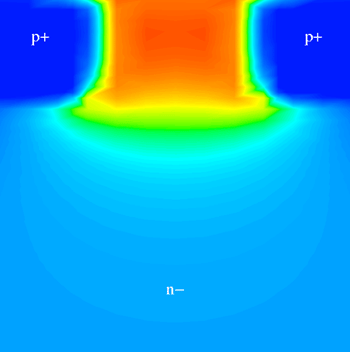
The most common doping impurities in SiC have activation energies
larger than the thermal energy even at room temperature. Inequivalent
sites of SiC, one with cubic surrounding and the other with hexagonal
surrounding, cause site-dependent impurity levels. Therefore, an
appropriate incomplete ionization model which accounts for ionization
level dependence on polytype and lattice sites is implemented. A
variety of other SiC-specific models, including band structure and
bandgap narrowing; Shockley-Read-Hall and Auger recombination,
temperature- and field-dependent impact ionization; and mobility
dependencies on impurity concentration, lattice temperature, carrier
concentration, carrier energy, parallel and perpendicular electric
fields have been implemented.
The models are tested on state-of-the-art SiC rectifiers, switches, and
RF transistors. Three classes of SiC rectifiers were investigated: the
Schottky barrier diodes which offer extremely high switching speed but
suffer from high leakage current; the PiN diodes which offer low
leakage current but show reverse recovery charge during switching and
have a large junction forward voltage drop due to the wide bandgap of
SiC; and the merged PiN Schottky diodes which offer Schottky-like
on-state and switching characteristics and PiN-like off-state
characteristics.
Three types of unipolar transistors were simulated. UMOSFET devices,
which were the first unipolar transistors realized in SiC, have shown
good on- and off-state characteristics but suffered from problems
including lower inversion layer mobility and high electric field
crowding at its trench corners. The DMOSFET structure formed by using a
double ion implantation has avoided the trench problems occurred in
UMOSFET, but still has low inversion layer mobility. An ACCUFET
structure is proposed by incorporating an n-type counter-doped layer
along the oxide/semiconductor interface to restore the low inversion
layer mobility observed at both UMOSFET and DMOSFET.
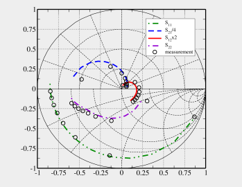
The implemented models were further tested on RF transistors. A
microwave MESFET fabricated using epitaxial layers on semi-insulating
SiC substrates was investigated for both DC and high frequency
characteristics. The results of the simulation were compared to
measurements, and excellent agreement was obtained.
|