|
Highly integrated
microelectronic circuits such as microprocessors require dense
interconnects with dimensions down to some 100 nm. With the resulting
increase in current density, electromigration-induced failure becomes a
more and more challenging issue. Significant advances have been made by
choosing copper instead of aluminum as an interconnect metal, because
copper has an improved electromigration bulk resistance. On the other
hand, low copper affinity introduces high diffusivity paths along
copper/barrier interfaces and thereby promotes nucleation of intrinsic
voids.
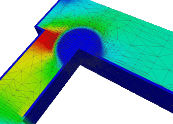
The design of an electromigration-compatible interconnect layout is a
complex task which cannot be handled using simplistic design rules.
There is a lot of theoretical work available for explaining and
modeling the manifold physical phenomena behind electromigration, but
only very small parts of it were actually implemented in software tools
and tested on real-world applications in order to support the work of
interconnect layer designers.
Electromigration is an atomic transport process which results from
momentum transfer to the constituent metal atoms due to collisions with
conduction electrons. As atoms electromigrate, there is a depletion of
material "upstream" and an accumulation "downstream" at sites of
flux divergence. This can lead to the formation and growth of voids at
points of material depletion, causing a large increase in electrical
resistance. On the other hand, accumulation of material may cause
dielectric cracking and the formation of an extrusion, resulting in a
short circuit between adjacent lines.
The development of intrinsic voids which lead to interconnect failure
goes through two distinct phases. These phases exhibit not only
different influences on the operating ability of the interconnect but
are also based on different physical processes. The first phase is the
void nucleating phase. In this phase no electromigration-generated
voids are present, and there is no significant resistance change. The
second phase begins when a void is nucleated and visible in SEM
pictures. This is the rapid phase of failure development. The void
expands from its initial position (nucleation site) to a size which can
significantly change the resistance or completely severe the
connection.
In our work we evaluate state-of-the-art theoretical work, improve weak
points, bridge the missing links, develop a widely applicable
interconnect reliability characterization tool, and verify it on real-world
applications.
|