|
The shrinking of gate
dielectric thicknesses of submicron CMOS transistors makes the use of
alternative gate dielectrics such as ZrO2 necessary. These materials,
however, suffer from high defect densities. Therefore, gate dielectric
reliability becomes a crucial issue not only for non-volatile memories
but even for logic applications. While the current transport through
high-k dielectric layers either by direct or defect-assisted tunneling
has been studied intensely applying sophisticated methods, the modeling
of dielectric breakdown has been investigated only recently. These
processes are usually modeled independently, although they are
physically directly related, since the time-to-breakdown of a gate
dielectric depends on the injected charge. A set of models has been
developed which directly links the simulation of direct and
trap-assisted leakage current with the creation and occupation of traps
and the occurence of breakdown.
We distinguish three processes which happen sequentially and finally
trigger breakdown. Assuming an ideally virgin dielectric, the direct
tunneling current through the dielectric layer gives rise to the
creation of neutral defects. This gate leakage is modeled as the sum of
two processes, direct and trap-assisted tunneling. Assuming a fresh and
defect-free dielectric layer, only direct tunneling is present, which
is
modeled following the commonly applied Tsu-Esaki model. The created
defects give rise to trap-assisted tunneling, leading to the occupation
of the traps by electrons and to the creation of new defects. The
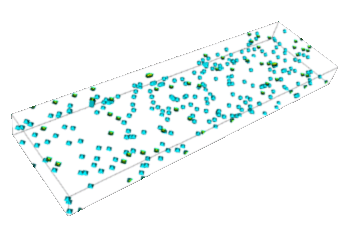
location of the traps is assumed to be random within the dielectric
layer, as shown in the figure, while a constant energy level is
assumed. As soon as such a percolation path is created, the dielectric
layer loses its insulating behavior and the current suddenly increases.
The implementation of these models into the device simulator Minimos-NT
allows the two- and three-dimensional study of the gate dielectric
degradation process.
Further work was devoted to the study of quasi-bound state tunneling,
the modeling of carrier transport in carbon nanotube devices, and the
development of VSP, the Vienna
Schrödinger-Poisson solver.
|