, which is
suspected to have a strong impact on hole capture processes in NBTI and
has therefore been phenomenologically introduced in the two-stage model
(TSM) [61].
, which is
suspected to have a strong impact on hole capture processes in NBTI and
has therefore been phenomenologically introduced in the two-stage model
(TSM) [61].
The concept of NMP has been used in a slightly modified variant termed
multiphonon field-assisted tunneling (MPFAT) [116, 115, 116, 117, 125, 55], which
was proposed for ionization of deep impurity centers. The underlying theory accounts
for the fact that the emission of charge carriers out of bulk traps is accelerated in the
presence of an electric field. This effect is eventually related to the shortened
tunneling distance through a triangular barrier when considering thermal
excitation of the charge carriers. According to theoretical calculations of
Ganichev et al. [117], it yields a field enhancement factor , which is
suspected to have a strong impact on hole capture processes in NBTI and
has therefore been phenomenologically introduced in the two-stage model
(TSM) [61].
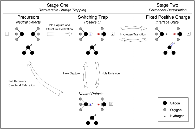
The TSM relies on the Harry-Diamond-Laboratories (HDL) [15] model but is
extended by a second stage accounting for the permanent component of NBTI (cf.
Fig. 6.3). The defect precursor, an oxygen vacancy according to the HDL model, is
capable of capturing substrate holes via the aforementioned MPFAT mechanism. The
trap level  of the precursor is located below the substrate valence band and
subject to a wide distribution due to the amorphousness of
of the precursor is located below the substrate valence band and
subject to a wide distribution due to the amorphousness of  . Upon hole
capture, the defect undergoes a transformation to an
. Upon hole
capture, the defect undergoes a transformation to an  center, which is visible in
ESR measurements [43]. In this new configuration, it features a
center, which is visible in
ESR measurements [43]. In this new configuration, it features a  dangling bond
associated with a defect level
dangling bond
associated with a defect level  within or close to within the substrate bandgap
in accordance to [162]. The level shift from
within or close to within the substrate bandgap
in accordance to [162]. The level shift from  to
to  arises from the change to
a new ‘stable’ defect configuration, namely the
arises from the change to
a new ‘stable’ defect configuration, namely the  dangling bond. In the
  center configuration, the defect can be repeatedly charged and discharged by
electrons tunneling in or out of its dangling bond. The associated switching
behavior1
is in agreement with the experimental observations made in electrical
measurements [15, 16]. Only in the neutral state
center configuration, the defect can be repeatedly charged and discharged by
electrons tunneling in or out of its dangling bond. The associated switching
behavior1
is in agreement with the experimental observations made in electrical
measurements [15, 16]. Only in the neutral state  , in which the
  dangling bond
is doubly occupied by an electron, the
dangling bond
is doubly occupied by an electron, the  center can be annealed, thereby becoming
an oxygen vacancy again.
center can be annealed, thereby becoming
an oxygen vacancy again.
 and
and  . From
the neutral charge state
. From
the neutral charge state  , the defect can undergo structural relaxation over a
thermal barrier and arrives at its initial configuration. The second stage gives
an explanation for the permanent component, which is attributed to a hydrogen
transition from state
, the defect can undergo structural relaxation over a
thermal barrier and arrives at its initial configuration. The second stage gives
an explanation for the permanent component, which is attributed to a hydrogen
transition from state  to
to  . This transition fixes the positive charge (red
plus sign) in the defect and creates a new interface state (ellipse with one or
two blue arrows).
. This transition fixes the positive charge (red
plus sign) in the defect and creates a new interface state (ellipse with one or
two blue arrows).The second stage involves an amphoteric trap, most probably a  center, which
has been found to interact with the switching trap as observed in irradiation
experiments [43]. That is, a hydrogen is detached from an interfacial
center, which
has been found to interact with the switching trap as observed in irradiation
experiments [43]. That is, a hydrogen is detached from an interfacial  -
- bond
and leaves behind a
bond
and leaves behind a  center. In a subsequent reaction, it saturates the
dangling bond of the
center. In a subsequent reaction, it saturates the
dangling bond of the  center. This stage fixes the positive charge at
the oxide defect and creates a new interface state, whose charge state is
controlled by the substrate Fermi level. Since the hydrogen transition is
assumed to last much longer than the hole capture or emission process, this
stage corresponds to the permanent or slowly recoverable component of
NBTI.
center. This stage fixes the positive charge at
the oxide defect and creates a new interface state, whose charge state is
controlled by the substrate Fermi level. Since the hydrogen transition is
assumed to last much longer than the hole capture or emission process, this
stage corresponds to the permanent or slowly recoverable component of
NBTI.
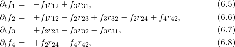
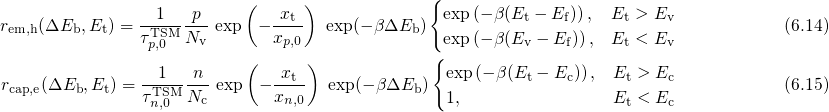
Mathematically, the dynamics of this complex mechanism are described by the set of the following rate equations:
The subscript of
of  stands for the state according to the numbering in Fig. 6.3.
The transition rates are denoted as
stands for the state according to the numbering in Fig. 6.3.
The transition rates are denoted as  , with
  and
and  as the initial and the final
states, respectively. The rate
as the initial and the final
states, respectively. The rate  is derived from the SRH equations (2.69),
in which the empirical enhancement factor
is derived from the SRH equations (2.69),
in which the empirical enhancement factor  for the MPFAT
transition2
for the MPFAT
transition2
 has been phenomenologically introduced. Then the transition rates read
with The quantity
has been phenomenologically introduced. Then the transition rates read
with The quantity  is the equivalent of
  in the TSM and can be calculated
according to equation (2.76). The barriers
in the TSM and can be calculated
according to equation (2.76). The barriers  and
and  are defined
analogously to the barrier
are defined
analogously to the barrier  in Fig. 2.5. Therefore, they corresponds to the
barrier component, which must be overcome in both directions of the transitions
in Fig. 2.5. Therefore, they corresponds to the
barrier component, which must be overcome in both directions of the transitions
 and
and  , respectively (cf. Fig 2.5). For the transitions between the states
 and
and  the capture and emission of electrons as well as holes are taken into account.
 ) is represented by the rate
  , which is
modeled by a structural relaxation over a thermal barrier
, which is
modeled by a structural relaxation over a thermal barrier  .
. 
 denotes the attempt frequency, which is usually in the order of
  . The
hydrogen transition
. The
hydrogen transition  is modeled assuming a field-dependent thermal barrier, as
shown in Fig. 6.4.
is modeled assuming a field-dependent thermal barrier, as
shown in Fig. 6.4. 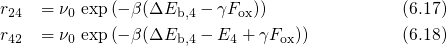
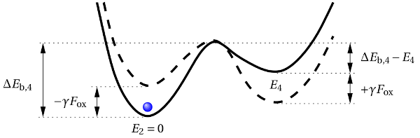
 ) but lowers that of state 4 (
 ). Since the interfacial
 -
- bonds are associated with a dipole moment, the shift of the energy
minima depends linearly on the oxide field with a proportionality constant of
bonds are associated with a dipole moment, the shift of the energy
minima depends linearly on the oxide field with a proportionality constant of
 . The applied oxide field gives rise to a reduced forward barrier (
 ) and
an increased reverse barrier (
) and
an increased reverse barrier ( ). Without loss of generality, the value of
 is set to zero.
The following simulations are based on the same numerical scheme as has
been presented in Section 3.2 and are used for the ETM and the LSM in
Chapter 4 and 5. Each representative trap in this scheme is characterized by its
individual set of defect levels and barriers. The generated random numbers are
homogeneously distributed for  ,
,  ,
,  , and
, and  while they follow a
Fermi-derivative (Gaussian-like) distribution [90] for
while they follow a
Fermi-derivative (Gaussian-like) distribution [90] for  and
and  . The
remaining quantities including
. The
remaining quantities including  ,
,  ,
,
 ,
,  , and
, and  are assumed to be
single-valued.
are assumed to be
single-valued.
In contrast to previous models, oxide charges (state 2) as well as interface traps
(state 4) are incorporated into the TSM so that two states must be considered for
the calculation of  . It is important to note that only a part of the
overall degradation during stress is observed within the experimental time
window. As demonstrated in Fig. 6.5, a large fraction already occurs before the
beginning of the OTF measurement (
. It is important to note that only a part of the
overall degradation during stress is observed within the experimental time
window. As demonstrated in Fig. 6.5, a large fraction already occurs before the
beginning of the OTF measurement ( ) and only a part of the
  degradation can be monitored by this technique (cf. Section 1.3.2). As a
consequence, the measured threshold voltage shift must be calculated as
degradation can be monitored by this technique (cf. Section 1.3.2). As a
consequence, the measured threshold voltage shift must be calculated as

 so that
only the tails of the real recovery curve can be assessed experimentally.
so that
only the tails of the real recovery curve can be assessed experimentally.
 shift from the recorded drain current during the relaxation
phase. Note that OTF only assesses the change of threshold voltage referred to
the first measurement point, but disregards the degradation accumulated before.
Analogously, the NBTI recovery may start already before
shift from the recorded drain current during the relaxation
phase. Note that OTF only assesses the change of threshold voltage referred to
the first measurement point, but disregards the degradation accumulated before.
Analogously, the NBTI recovery may start already before  but the MSM
technique can only monitor the tails of the degradation curves.
but the MSM
technique can only monitor the tails of the degradation curves.The TSM [61] has been compared to a large set of measurement data, including
various combinations of stress voltages and temperatures. For illustration, a fit to the
eMSM (cf. Section 1.4) data at  is depicted in Fig. 6.6. The findings of this
model are evaluated in the following:
is depicted in Fig. 6.6. The findings of this
model are evaluated in the following:
 ) is determined and no sign of saturation appears until
  .
Detrapping during relaxation extends over the whole experimental time
window ranging from
.
Detrapping during relaxation extends over the whole experimental time
window ranging from  to
to  .
.
 follows a logarithmic time behavior during the whole stress
phase.
follows a logarithmic time behavior during the whole stress
phase.
 where the
  curve starts to level off. This is
due to the fact that the TSM also accounts for the permanent component
of NBTI.
curve starts to level off. This is
due to the fact that the TSM also accounts for the permanent component
of NBTI.
 during the stress and the relaxation phase
exhibit a ratio of
during the stress and the relaxation phase
exhibit a ratio of  in agreement with [61]. This asymmetry is
demonstrated by the temporal change of the trap occupancy in Fig. 6.6 (right).
After the level shift from
in agreement with [61]. This asymmetry is
demonstrated by the temporal change of the trap occupancy in Fig. 6.6 (right).
After the level shift from  to
to  , when the defect transforms from an
oxygen vacancy to an
, when the defect transforms from an
oxygen vacancy to an  center, the trap level
  lies closer to the
substrate valence bandedge than
lies closer to the
substrate valence bandedge than  . This results in higher trapping rates
for hole capture (
. This results in higher trapping rates
for hole capture ( ) and emission (
 ) so that the subsystem
of states
) so that the subsystem
of states  and
and  is only weakly affected by
  during recovery.
Therefore, this reduced system is close to equilibrium, meaning that
during recovery.
Therefore, this reduced system is close to equilibrium, meaning that

 . Then the occupation
  is given by and can be interpreted as the electron occupancy
  of the
  center with
the defect level
center with
the defect level  . According to the above equation, the defect occupancy in
the whole defect system of the TSM follows the substrate Fermi level, which
thus controls the annealing rate
. According to the above equation, the defect occupancy in
the whole defect system of the TSM follows the substrate Fermi level, which
thus controls the annealing rate  and can slow down the recovery. Due to
this ‘occupancy effect’, the TSM is able to capture the asymmetry between
stress and relaxation.
and can slow down the recovery. Due to
this ‘occupancy effect’, the TSM is able to capture the asymmetry between
stress and relaxation.
 device (symbols) for 8 different stress voltages at a
temperature of
device (symbols) for 8 different stress voltages at a
temperature of  . The field acceleration as well as the asymmetry between
stress and relaxation have been nicely reproduced. Right: Averaged trap
occupancy during stress and recovery for a single trap. The dotted lines refer
to oxide defects in state
. The field acceleration as well as the asymmetry between
stress and relaxation have been nicely reproduced. Right: Averaged trap
occupancy during stress and recovery for a single trap. The dotted lines refer
to oxide defects in state  or
or  , while the solid lines include the positively
charged defects (state
, while the solid lines include the positively
charged defects (state  ) only. The ratio between the slope of the stress (
 )
and the relaxation (
)
and the relaxation ( ) curve yields
  , as observed experimentally
in [61].
, as observed experimentally
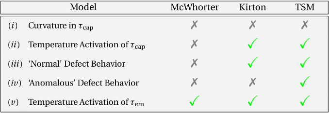
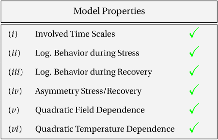
in [61].The TSM is found to satisfy all criteria of Table 6.2 and therefore seems to properly
describe NBTI degradation. Besides that, it also agrees well with the observation of a
field-dependent recovery, which is demonstrated by the measurements shown in
Fig. 6.7. Due to the occupancy effect, the substrate Fermi level  controls the
portion of neutral
controls the
portion of neutral  centers (state 3) which can return to state
  by structural
relaxation and contribute to the NBTI recovery. Interestingly, this field dependence is
compatible with the finding that the emission times of ‘anomalous defects’ are
field-sensitive.
by structural
relaxation and contribute to the NBTI recovery. Interestingly, this field dependence is
compatible with the finding that the emission times of ‘anomalous defects’ are
field-sensitive.
 under the same conditions (
 ,
,  ). The following
recovery phase (left and right panel) was interrupted for a period of time during
which
). The following
recovery phase (left and right panel) was interrupted for a period of time during
which  was switched from the recovery voltage of
  to
to  for
for
 (middle panel). The experimental data are marked by symbols, while the
simulations are represented by lines (dotted:
(middle panel). The experimental data are marked by symbols, while the
simulations are represented by lines (dotted:  , solid:
  due to
 , dashed:
  due to
  ). The measurements demonstrate
that the recovery is clearly affected by variations of the recovery bias. This
effect is reminiscent of the field-dependent emission times seen in TDDS. The
agreement of the simulations with the measurements shows that the TSM can
explain the field-dependent NBTI recovery.
). The measurements demonstrate
that the recovery is clearly affected by variations of the recovery bias. This
effect is reminiscent of the field-dependent emission times seen in TDDS. The
agreement of the simulations with the measurements shows that the TSM can
explain the field-dependent NBTI recovery.The distributions of trap levels obtained from the model calibration are depicted in
Fig. 6.8. The trap levels  of the precursors (state
  ) are uniformly distributed
between
) are uniformly distributed
between  and
and  in qualitative agreement with the values in [39].
The defects located the highest have also the highest substrate hole capture rates
in qualitative agreement with the values in [39].
The defects located the highest have also the highest substrate hole capture rates
 and therefore have already been transformed
  centers (states
  and
and  )
after a stress time of
)
after a stress time of  . In this new configuration, they feature a trap
level
. In this new configuration, they feature a trap
level  in the range between
  and
and  in qualitative
agreement with the values published in [39]. According to equation (6.21), the
occupancy of the
in qualitative
agreement with the values published in [39]. According to equation (6.21), the
occupancy of the  levels is determined by the substrate Fermi energy
and thus the number of neutralized defects in the
levels is determined by the substrate Fermi energy
and thus the number of neutralized defects in the  center configuration
(state
center configuration
(state  ) increases with a lower energies. Since only defects in this state
transformed to a precursor (state
) increases with a lower energies. Since only defects in this state
transformed to a precursor (state  ) again, the number of traps in state
  diminished towards the substrate Fermi energy (cf. Fig. 6.8). The donor
levels of the interface states have been assumed to be uniformly distributed
and are located within the lower part of the substrate bandgap consistent
with [64].
diminished towards the substrate Fermi energy (cf. Fig. 6.8). The donor
levels of the interface states have been assumed to be uniformly distributed
and are located within the lower part of the substrate bandgap consistent
with [64].
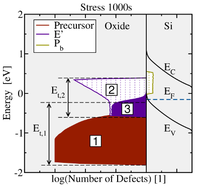
 . The numbers in the white filled boxes denote the state of the defects.
The area in the plain red color gives the number of precursors (state
. The numbers in the white filled boxes denote the state of the defects.
The area in the plain red color gives the number of precursors (state  ) with
the trap level
) with
the trap level  . The rest of the defects is in the
  center configuration,
in which they can be positively charged (purple striped pattern) or neutralized
(plain purple color) and have a trap level of
center configuration,
in which they can be positively charged (purple striped pattern) or neutralized
(plain purple color) and have a trap level of  . The occupied (plain) and
unoccupied (striped) interface states are depicted as beige areas. The beige
striped area gives the density of interface states originating from the
. The occupied (plain) and
unoccupied (striped) interface states are depicted as beige areas. The beige
striped area gives the density of interface states originating from the  centers.
So far, classical calculations of the band diagram have been performed to obtain the
interface quantities, such as the position of the bandedges ( ,
,  ), the Fermi
level (
), the Fermi
level ( ), and the electric field (
 ) within the dielectric. These quantities enter
the expressions of the rates and will significantly alter them due to their exponential
dependences. However, the SRH rates (6.9) used in Section 6.3.1 are valid for a
three-dimensional electron gas [55] but this assumption breaks down for an
inversion layer of MOS structures. In the one-dimensional triangular potential
well in the channel, quasi-bound states build up and form subbands, which
correspond to the new initial or final energy levels for the charge carriers
undergoing an NMP transitions. The quantum mechanical transition rates are
obtained following the derivation in Section 2.5.2 but using the DOS for
one-dimensionally confined holes. Then the rate equation (2.59) modifies to
) within the dielectric. These quantities enter
the expressions of the rates and will significantly alter them due to their exponential
dependences. However, the SRH rates (6.9) used in Section 6.3.1 are valid for a
three-dimensional electron gas [55] but this assumption breaks down for an
inversion layer of MOS structures. In the one-dimensional triangular potential
well in the channel, quasi-bound states build up and form subbands, which
correspond to the new initial or final energy levels for the charge carriers
undergoing an NMP transitions. The quantum mechanical transition rates are
obtained following the derivation in Section 2.5.2 but using the DOS for
one-dimensionally confined holes. Then the rate equation (2.59) modifies to
 does not enter this derivation
and consequently the DOS can be expressed as
does not enter this derivation
and consequently the DOS can be expressed as 
 can be identified as
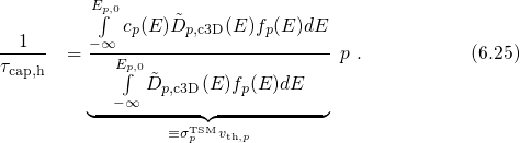
 (cf. Fig. 6.9).

 corresponds to the first bound state. Inserting the modified cross section
in equation (2.65) and (2.66) yields and
corresponds to the first bound state. Inserting the modified cross section
in equation (2.65) and (2.66) yields and 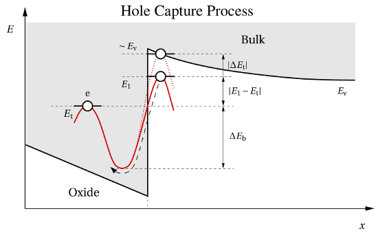
 when quantum confinement
is taken into account. The shift of the initial energy level from
when quantum confinement
is taken into account. The shift of the initial energy level from  to
to  reduces the corresponding NMP barriers (red lines) and thus enhances the hole
capture rates. Note that the energy difference between
reduces the corresponding NMP barriers (red lines) and thus enhances the hole
capture rates. Note that the energy difference between  and
and  varies with
the oxide field and thus affects the field dependence of
varies with
the oxide field and thus affects the field dependence of  and
and  .
.These rates have been used to incorporate the aforementioned quantum effects into
the TSM, which has been evaluated against the same set of experimental data. For a
proper comparison with the classical variant of TSM, only the NMP parameters
( ,
,  ,
,  , and
, and  ) have been optimized while all other parameters
have been held fixed. The simulated degradation curves show a good agreement with
experimental data (see Fig. 6.10) so that the quantum mechanically refined variant
of the TSM still fulfills all criteria listed in Table 6.2. It is noted here that
these simulations yield an the uppermost trap levels
) have been optimized while all other parameters
have been held fixed. The simulated degradation curves show a good agreement with
experimental data (see Fig. 6.10) so that the quantum mechanically refined variant
of the TSM still fulfills all criteria listed in Table 6.2. It is noted here that
these simulations yield an the uppermost trap levels  , which have been
shifted downwards by about the same energy as the separation of
, which have been
shifted downwards by about the same energy as the separation of  and
and
 (ranging between
  and
and  ). This can be explained when
considering that, first,
). This can be explained when
considering that, first,  is replaced
  in the rate equations (6.27) and
(6.28) and, second, the NMP barrier for hole capture is reduced by this
energy difference. From this it follows that also the trap levels
in the rate equations (6.27) and
(6.28) and, second, the NMP barrier for hole capture is reduced by this
energy difference. From this it follows that also the trap levels  must
be shifted down by approximately the same energy in order to obtain hole
capture rates of an equal magnitude. In summary, it has been assured that
also the quantum mechanically refined variant of the TSM can explain the
NBTI data and must therefore be considered as a reasonable NBTI model.
must
be shifted down by approximately the same energy in order to obtain hole
capture rates of an equal magnitude. In summary, it has been assured that
also the quantum mechanically refined variant of the TSM can explain the
NBTI data and must therefore be considered as a reasonable NBTI model.
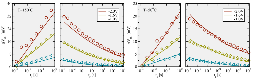
 is
subjected to two different temperatures (
is
subjected to two different temperatures ( left panels,
  tight
panels) and three different gate voltages for
tight
panels) and three different gate voltages for  during the first phase termed
trapping/stress (left hand side). After the gate voltage is removed, the second
phase called detrapping/relaxation phase (right-hand side) sets in. Symbols
mark measurement data while solid lines belong to simulation data. Note that
the temperature and field dependence is well reproduced simultaneously for
relaxation phase. The slight tendency of the simulations to underestimate the
measurements at high stress temperatures during the stress phase appear in
the classical as well as in the quantum mechanical simulations. They may be
traced back to the mobility degradation of the drain current during the MSM
measurements [26].
during the first phase termed
trapping/stress (left hand side). After the gate voltage is removed, the second
phase called detrapping/relaxation phase (right-hand side) sets in. Symbols
mark measurement data while solid lines belong to simulation data. Note that
the temperature and field dependence is well reproduced simultaneously for
relaxation phase. The slight tendency of the simulations to underestimate the
measurements at high stress temperatures during the stress phase appear in
the classical as well as in the quantum mechanical simulations. They may be
traced back to the mobility degradation of the drain current during the MSM
measurements [26].The criteria in Table 4.1 have been successfully satisfied by the TSM. With this
respect, the TSM should be regarded as model qualified to describe NBTI. However,
these criteria only evaluate the degradation produced by an ensemble of defects but
do not consider whether the behavior of a single defect is correctly reproduced. For
this reason, the TSM will be investigated using the time constant plots in the
following. Since the TDDS measurements cannot capture the permanent component
of NBTI, the transition state diagram must be reduced to stage one. This means that
the equation (6.8) and the rates  and
and  in equation (6.6) must be omitted.
Since the trap level
in equation (6.6) must be omitted.
Since the trap level  is assumed to lie closer to the valence band edge
than
is assumed to lie closer to the valence band edge
than  , the accociated rate
  and
and  are much larger than
  .
Thus the fast switching between state
.
Thus the fast switching between state  and
and  produces noise, which is
undesired for the analysis of
produces noise, which is
undesired for the analysis of  in the time constant plots. Therefore, a
compact rate expression for the transition
in the time constant plots. Therefore, a
compact rate expression for the transition  is sought. One can
calculate the corresponding emission time
is sought. One can
calculate the corresponding emission time  as the mean first passage time
in continuous time Markov chain theory [131] (discussed in Section 3.2).
as the mean first passage time
in continuous time Markov chain theory [131] (discussed in Section 3.2).

 and
and  , the above expression can be simplified to
 ,
,
 , and
, and  can be neglected. This reduced variant of the TSM is fitted against the TDDS data and will be
evaluated according to the list of criteria established in Section 1.3.4.
can be neglected. This reduced variant of the TSM is fitted against the TDDS data and will be
evaluated according to the list of criteria established in Section 1.3.4.
 in the time constant plot of Fig. 6.11 has a wrong
curvature. This can be traced back to the fact that
in the time constant plot of Fig. 6.11 has a wrong
curvature. This can be traced back to the fact that  is proportional
to
is proportional
to  according to equation (6.31).
 .
.
 as demonstrated in Fig. 6.11.
However, this is only true for defects with a trap level
as demonstrated in Fig. 6.11.
However, this is only true for defects with a trap level  above
above
 . In this case,
  approximates to
  and
and  is given by
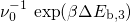 .
.
 if
if  is located slightly
below
is located slightly
below  at the relaxation voltage. Then the field dependence is caused
by the term
at the relaxation voltage. Then the field dependence is caused
by the term  in equation (6.32).
 is thermally-activated.
 , the
TSM can explain both defect behaviors. However, it does not give the correct
curvature of
, the
TSM can explain both defect behaviors. However, it does not give the correct
curvature of  due to the field enhancement factor.
As demonstrated in the previous section, the TSM is indeed an important
improvement of the NBTI model. Regarding the time constant plots (cf. Table 6.3),
the introduction of the state  gives an explanation for ‘normal’ as well
as the ‘anomalous’ defect behavior. However, the TSM predicts a wrong
curvature of
gives an explanation for ‘normal’ as well
as the ‘anomalous’ defect behavior. However, the TSM predicts a wrong
curvature of  and thus cannot be reconciled with the TDDS data. As a
consequence, it can be concluded that the TSM performs well for stress
and relaxation curves but fails to describe the behavior of single defects.
and thus cannot be reconciled with the TDDS data. As a
consequence, it can be concluded that the TSM performs well for stress
and relaxation curves but fails to describe the behavior of single defects.