

Degradation of Electrical Parameters of Power Semiconductor Devices – Process Influences and Modeling
4.4 Assessment of the extrapolation model
The model for the increase of the device temperature with power supplied to the heater proposed above must be validated. Within the range of the temperature of the thermal chuck the approach can be tested experimentally. Outside this range the extrapolation can be compared to thermal FEM simulations which are capable of handling non-linear thermal resistances. Such simulations give an approximate temperature distribution by transferring the partial differential heat equation to linear equations and solving them numerically.
4.4.1 Experimental
Within the chuck temperature range the extrapolation methods (4.7) and (4.8) can be compared with experimental data as shown in Fig. 4.9.

 [PobegenTDMR13]. The lines are the estimations of
  for linear (4.8) and exponential (4.7)
extrapolation.
for linear (4.8) and exponential (4.7)
extrapolation.
The exponential extrapolation method can correctly capture the increase of the device temperature with heater power. In order to resolve the correctness of the approach better, Fig. 4.10 shows the relative error of the two methods over the switched temperature range.

The error of the linear method rises with temperature difference while the error of the exponential method stays below a few percent.
The exponential extrapolation method includes the thermal resistance between the wafer and the chuck or between the die and the package. Consequently, the method can also be used to estimate the temperature of a device which is thermally decoupled from a heat sink. This allows reaching even higher temperatures in the device because only the inefficient mechanisms radiation and convection cause a reduction of the device temperature. For wafer tests thermal decoupling can be achieved by placing the wafer on a plastic layer or by inserting small area spacers between the wafer and the chuck. This approach considerably increases the accessible temperature range, as shown in Fig. 4.11.

Consequently, also semiconductor materials which have a low thermal resistivity, as e.g. four layer hexagonal SiC (4H-SiC), which has about 40 % of the thermal resistivity of Si, can be operated at high temperatures with the poly-heater.
4.4.2 Thermal simulations
In a first attempt to model the increase of the device temperature with the power supplied to the poly-heater a two-dimensional (2D) thermal model was created using the commercially available analysis system (Ansys) FEM software by Ansys Incorporated. With this model an overall match with experimental data as shown in Fig. 4.12 could only be obtained by arbitrarily changing the thermal conductivity of the Si substrate and its temperature dependence.

with heater power. The original temperature dependent thermal conductivity values of the materials of the model cannot capture the dependence. Only by changing the material parameters arbitrarily a good match can be obtained.
The extrapolation of such a simulation to high temperatures is not of particular interest because it is mostly determined by the effective thermal conductivity at high temperatures. That is to say, the simulation depends on the same assumptions as the exponential extrapolation method which should be tested. In order to exempt the simulation from the same assumptions a 3D model was implemented where both the current through the heater and the heat spread was calculated [PobegenTDMR13]. For this model the structure as sketched in Fig. 4.1 was simplified by omitting the metal wires. Consequently, the model consists basically of two bricks of poly surrounded by SiO2 , and situated on a large block of Si.
To correctly capture the poly-heater behavior, the poly lines were simulated electrically and thermally. For the other materials of the model it was sufficient to perform only a thermal simulation, i.e. no electrical device simulation was conducted. The
temperature dependent electrical resistivity of the poly was obtained on a dedicated test structure on the same wafer. The temperature dependent thermal resistivity of the Si substrate was measured externally on an unprocessed raw wafer with a
calibrated differential scanning calorimetry equipment. The value of the thermal resistivity is rather large compared to standard Si [Let+87; GS64] because of the high doping level of the substrate [Sla64; LA05], needed to reduce the on-resistance of vertical power devices residing on the same wafer. The temperature dependence of the thermal resistivity could be modeled better with
a power law coefficient of  , instead of the suggested coefficient of
  [Let+87]. Also, a cross check of the change of the simulation result with a modification of the power law coefficient between
  and
and  showed vanishing influence. That is to say, in a small range the particular choice of the power law coefficient is rather irrelevant and
  eases the calculations considerably.
The model has Neumann boundary conditions at all borders except at the bottom surface. Those boundaries act as adiabatic boundaries meaning that heat flow through the boundary is prohibited. At the bottom a phenomenological layer was
introduced which accounts for the thermal behavior of the interface between the wafer and the chuck [PobegenTDMR13; CS01; IR05]. This layer is 20 µm thick and has a thermal conductivity of 0.5 W/(m K). The bottom surface of this interface layer was set to
Dirichlet boundary conditions with the temperature of the chuck. A  mm large Si block was needed to account for the large lateral heat spread visible in an increase of the surface temperature at the outer boundaries. The device temperature was determined by averaging the temperature of the Si
substrate near the interface to the SiO2 at the exact position of the device.
mm large Si block was needed to account for the large lateral heat spread visible in an increase of the surface temperature at the outer boundaries. The device temperature was determined by averaging the temperature of the Si
substrate near the interface to the SiO2 at the exact position of the device.
In Fig. 4.13 a comparison between the simulation result and the exponential extrapolation method is shown.

The 3D FEM simulation tends to overestimate the device temperature slightly. This might be due to the fact that, even though the exact dimensions of the heater structure and accurate material parameters were simulated, possible cooling parts
were neglected. These are especially the power metal pads for device contact and the reduction of the actual wafer diameter from 200 mm to a mm block.
The equivalent behavior of the extrapolation using (4.7) and the 3D simulation shows that the reduction to a 1D problem is a valid approach for the poly-heater structure [PobegenTDMR13].
Furthermore, the simulation allows investigating the reason for the equivalence of  and
and  . As shown in Fig. 4.14, during poly-heater use (high heater supply power) as well as during calibration (low heater power) approximately the same
relative temperature distributions occur.
. As shown in Fig. 4.14, during poly-heater use (high heater supply power) as well as during calibration (low heater power) approximately the same
relative temperature distributions occur.
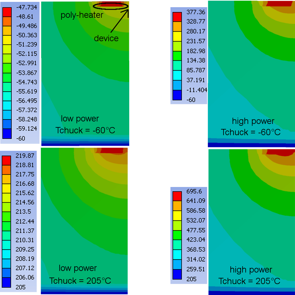
The region of the highest temperature is always very close to the device. Since the  of the substrate increases with temperature the same region is responsible for the thermal resistance. Consequently, the thermal resistance of the substrate is determined by the bottleneck region with the highest temperature close to the
device and both approaches to measure the thermal resistance give equivalent results.
of the substrate increases with temperature the same region is responsible for the thermal resistance. Consequently, the thermal resistance of the substrate is determined by the bottleneck region with the highest temperature close to the
device and both approaches to measure the thermal resistance give equivalent results.