« PreviousUpNext »Contents
Previous: 2.4 Setup for opto-electrical characterization Top: Home Next: 3.2 Impedance characteristics of GaN/AlGaN MIS structures
3 Methodologies for electrical characterization of interface defects in GaN–based MIS–HEMTs
Small signal investigations allow us to study in detail the behavior of the devices under test, as well as their frequency response. A number of methods based on impedance measurements have been established in the past decades in order to evaluate the density of defects at the interface with the dielectric. We focus on the two most used ones, explain their principle of operation and the approximations used, and we underline their limitations when applied to GaN–based devices. The main factor that makes such methods inaccurate in our case is the presence of the AlGaN layer. We investigate the role of the barrier and show that composite GaN/AlGaN structures require a more complex equivalent circuit model than that of regular MIS devices. Furthermore, we highlight other issues that constitute a challenge for an accurate characterization of MIS structures and MIS–HEMTs, namely hysteresis and the CV curve dependence on the measurement parameters. Finally, we develop two methods to evaluate the defect density based on the threshold voltage shift, applying a combination of small and large signal excitation.
3.1 The main established methods and their limitations
In this section we focus on the most used methods based on impedance measurements for the extraction of the interface defect density. In the first place, we need to develop a model for the small–signal response of a MIS structure. We present an equivalent circuit model, highlighting the assumptions and approximations used in the derivation. Then we describe the Terman and the conductance methods in detail, showing how they are applied to the experimental data and their limitations.
3.1.1 The equivalent circuit model
The model for the interface defects should describe the phenomenological loss of energy due to the trapping of conduction electrons into trap states. In the first place, the defects are effectively centres of charge storage: for this reason, we can associate to
them a certain capacitance  . Furthermore, charge trapping do not follow
precisely the AC signal, but it lags behind. The small–signal is a perturbation and the system evolves in time in order to return to equilibrium. This can be modelled with a certain characteristic time constant
. Furthermore, charge trapping do not follow
precisely the AC signal, but it lags behind. The small–signal is a perturbation and the system evolves in time in order to return to equilibrium. This can be modelled with a certain characteristic time constant  . The equivalent circuit model therefore
consists of the interface state capacitance in series with a certain resistance
. The equivalent circuit model therefore
consists of the interface state capacitance in series with a certain resistance  (series RC circuit), which gives rise to the time
constant given by the product
(series RC circuit), which gives rise to the time
constant given by the product  , as shown in Fig. 3.1a.
The equivalent circuit can be derived in a more rigorous way [63]: we summarize here the most important concepts and we highlight the approximations used. The net current density flowing in the device can be written as
![(3.1) \begin{equation} i (\mr {t}) = q \left [ r_n^c (\mr {t}) - r_n^e (\mr {t}) \right ] \label {rate_eq} \end{equation}](lateximages/lateximage-215.svg)
where  and
and  are the capture and emission rate constants for
electrons, respectively. The first assumption is the Shockley–Read–Hall (SRH) model for the rate constants. Originally, this theory has been developed for deep trap states inside a semiconductor, but its validity is here assumed to extended to interface states as
well. The rate constants depend on the density of electrons available at the semiconductor surface,
are the capture and emission rate constants for
electrons, respectively. The first assumption is the Shockley–Read–Hall (SRH) model for the rate constants. Originally, this theory has been developed for deep trap states inside a semiconductor, but its validity is here assumed to extended to interface states as
well. The rate constants depend on the density of electrons available at the semiconductor surface,  , the density of traps
  , the Fermi function
  and the probability for electron capture
  and emission
  as
as
![(3.2) \begin{equation} r_n^c (\mr {t}) = n_\mr {s} N_\mr {it} c_n \left [ 1 - f (\mr {t}) \right ] \quad \quad \mr {and} \quad \quad r_n^e (\mr {t}) =
N_\mr {it} e_n f (\mr {t}). \end{equation}](lateximages/lateximage-223.svg)
In the SRH model it is assumed that the capture and emission probability depend on the energy difference between the trap state and, in the case of electrons, the conduction band edge (this topic is discussed further in Chapter 4). In this case, we consider the
interface states to be located at the same energetic position inside the bandgap. We also assume the small–signal approximation to be valid, i.e., to a small variation  of the gate voltage around the mean value
  corresponds a small variation of the Fermi function and of the surface potential
  , according to

Finally, we assume that thermal equilibrium is reached, therefore the detailed balance equation is valid and we can write the electron emission probability as a function of the capture probability:

Manipulating Eq. (3.1) with these conditions, we can write a direct
relationship between the net current density and the variation of the surface potential, from which an equation for the admittance of the interface,  , can be derived:

The admittance can be modelled with a resistance and a capacitance in series, as shown in Fig. 3.1a. The response of the interface states is therefore characterized by the time constant  .
.


In order to investigate the defects at the interface with the dielectric, we need an equivalent circuit model for the full MIS structure. In the first place, we consider the distribution of charge in the device: the charge present at the gate contact  must be counterbalanced by the charge of the
depletion region of the semiconductor
must be counterbalanced by the charge of the
depletion region of the semiconductor  , the charge trapped at the interface
  and any possible fixed charge
  , according to

When the small signal is applied, only the quantities depending on the surface potential follow the bias oscillation. For this reason, the small–signal current density arises from the contribution of the depletion region,  , and that of the interface,
  . The former can be written as

and we have just derived an expression for the latter,  . Together, the small–signal current due to the variation of the surface potential is
![(3.8) \begin{equation} i (\mr {t}) = i_\mr {depl} (\mr {t}) + i_\mr {it} (\mr {t}) = \left [ Y_\mr {it} + i \omega \, C_\mr {diel} \right ] \delta \!\phi
_\mr {s}, \end{equation}](lateximages/lateximage-246.svg)
which corresponds to an equivalent circuit model of the depletion capacitance in parallel with the admittance of the interface states. As a second step, we consider the potential drop across the MIS structure. The small–signal bias applied to the gate,  , is distributed in the semiconductor and the
dielectric according to
, is distributed in the semiconductor and the
dielectric according to

We can evaluate the variation due to the small–signal by taking the time derivative of Eq. (3.9):

from which we can write
![(3.11) \begin{equation} \delta \!v (\mr {t})= \left [ \frac {1}{Y_\mr {it} + i \omega \;C_\mr {depl}} + \frac {1}{i \omega \;C_\mr {diel}} \right ] i (\mr
{t}). \end{equation}](lateximages/lateximage-250.svg)
The model of the full MIS device is therefore the parallel circuit of the depletion capacitance and the admittance of the interface states, in series with the dielectric capacitance. This is illustrated in Fig. 3.1b.
In the derivation of the admittance of the interface defects , we assumed all traps to be located at the same
position in the energy bandgap (single–level approximation). It is possible to extend this model to an ensemble of interface states distributed over a range of energy below the semiconductor conduction band. In this case, each level  contributes with its characteristic admittance
  , and the total admittance is the integral over all active states. In terms of our equivalent circuit model, we can model the ensemble of trap states as a parallel circuit of many single contribution
  , as shown in Fig. 3.1c.
Finally, we need to extract the quantity we are interested in, , from the measurement data. As mentioned in
Chapter 2, the result of an impedance measurement is a couple of real numbers that describe the complex impedance of the sample. For MIS structures we use a parallel model, which means that we measure the quantities  and
and  that define the complex admittance
  .
From this data it is easy to correct for the dielectric capacitance, which must be measured accurately and used as a parameter. In this way, we obtain the parallel capacitance and conductance
.
From this data it is easy to correct for the dielectric capacitance, which must be measured accurately and used as a parameter. In this way, we obtain the parallel capacitance and conductance  and
and  , and the equivalent model of the MIS structure is
shown in Fig. 3.1d. At this point, we can extract the interface defects admittance from our measurement using the
following equations:
, and the equivalent model of the MIS structure is
shown in Fig. 3.1d. At this point, we can extract the interface defects admittance from our measurement using the
following equations:

The first equation is the basis of the Terman method, which is discussed in Section 3.1.2. We already note that this approach requires to calculate the depletion capacitance, for which a theoretical model is needed. Also the doping profile must be known and
used as a parameter. In the case of an inhomogeneous doping, the calculation becomes more difficult and numerical methods might be necessary [64]. On the other hand, the conductance depends only on interface defects properties. is divided through the angular frequency in order
to obtain symmetric peaks as a function of frequency. The method based on the analysis of the conductance is described in Section 3.1.3.
3.1.2 The Terman or high frequency method
The goal of the Terman method is to extract the density of interface traps from the measurement of the CV of the device [65]. This technique relies on a major simplification of the model in Fig. 3.1b, known as the high frequency approximation, which consists of neglecting the admittance . In other words, we assume that the frequency is
so high that no trap responds to the AC signal during the sweep. The equivalent model is therefore a series of the dielectric capacitance and that of the depletion region only, whose capacitance  is given by

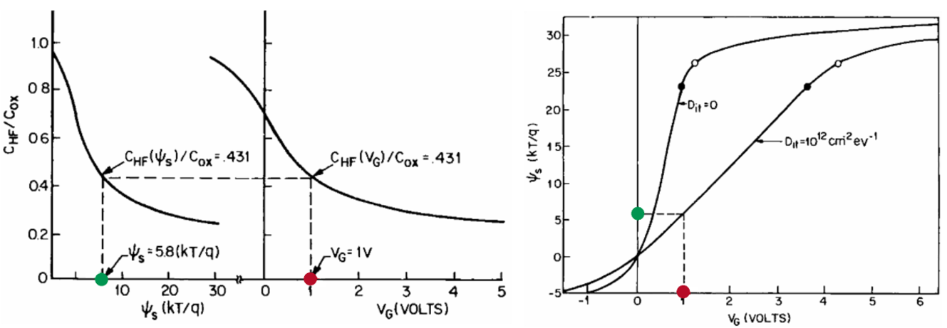

Figure 3.2: The simulated, ideal ( ) capacitance as a function of the surface po-
tential, in the high frequency approximation (a) and the measured CV curve,
) capacitance as a function of the surface po-
tential, in the high frequency approximation (a) and the measured CV curve,  (b). These two curves allow
us to calculate the real surface potential
(b). These two curves allow
us to calculate the real surface potential  , to be compared with the
ideal one (c), from which
, to be compared with the
ideal one (c), from which  can be extracted (from [38]).
In this case, the information about the interface defects can be indirectly extracted from the behavior of the semiconductor depletion capacitance [38]. In fact, this method is based on the comparison of the measurement with a simulated, ideal curve. The
capacitance of the depletion region and that of the interface states are functions of the band bending. It is possible to simulate the ideal curve in absence of trap states,  , from the device and
material properties [38]. Subsequently, from we can derive the
dependence of on with Eq. (3.13). An example is shown in Fig. 3.2a. The CV measurement provides the experimental curve , as shown in Fig. 3.2b. With such information we can extract the real surface potential as a function of the gate bias, as shown in the example of
Fig. 3.2c. We note that the presence of interface states results in a stretch–out with respect to the ideal curve.
, from the device and
material properties [38]. Subsequently, from we can derive the
dependence of on with Eq. (3.13). An example is shown in Fig. 3.2a. The CV measurement provides the experimental curve , as shown in Fig. 3.2b. With such information we can extract the real surface potential as a function of the gate bias, as shown in the example of
Fig. 3.2c. We note that the presence of interface states results in a stretch–out with respect to the ideal curve.
The density of interface states, , can be calculated from the data in Fig. 3.2. We consider again the charge balance in the MIS structure of Eq. (3.6). The voltage drop at the gate contact is the difference between the applied bias and the band bending of
the semiconductor, therefore the total charge can be written as

The charges of the depletion region and that of the interface traps are functions of the surface potential through their respective capacitances:

For a small change of the applied gate bias, we can write
![(3.16) \begin{equation} C_\mr {diel} \; \mr {d}V_\mr {gate} = \left [ C_\mr {diel} + C_\mr {it} \,(\phi _\mr {s}) + C_\mr {depl} \,(\phi _\mr {s}) \right
] \mr {d}\phi _\mr {s} \end{equation}](lateximages/lateximage-279.svg)
from which we derive an expression for the interface trap capacitance:

where is the simulated, ideal
curve of Fig. 3.2a, and the derivative  can be
calculated from Fig. 3.2c. This finally allows us to calculate the density of interface states as [38]
can be
calculated from Fig. 3.2c. This finally allows us to calculate the density of interface states as [38]

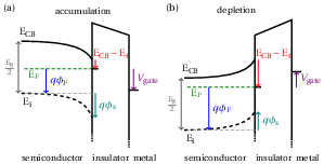
In order to determine the energy of the trap states, an additional assumption is necessary. According to the Terman method, only the traps aligned with the semiconductor Fermi level are considered to contribute to the stretch–out of the capacitance curve.
This would be possible only if the system under AC excitation reached a quasi–equilibrium situation, for which the position of the Fermi level remains constant and depends only on the value of the DC bias,  . In other words, we assume that only the
response of a trap located at
. In other words, we assume that only the
response of a trap located at  is in resonance with the
small–signal applied to the gate. Such an approximation neglects the contribution of the DC bias to the trapping events at the interface. As we will discuss in the following sections, this can indeed result in an incorrect interpretation of the activation energy of the
defects, and to an underestimation of the density of interface states. The energy diagram of this situation is shown in Fig. 3.3 for a n–type semiconductor in accumulation and depletion conditions.
is in resonance with the
small–signal applied to the gate. Such an approximation neglects the contribution of the DC bias to the trapping events at the interface. As we will discuss in the following sections, this can indeed result in an incorrect interpretation of the activation energy of the
defects, and to an underestimation of the density of interface states. The energy diagram of this situation is shown in Fig. 3.3 for a n–type semiconductor in accumulation and depletion conditions.

At each measurement point at a certain corresponds a value of the surface potential
, at which we can calculate the density of
interface traps with Eq. (3.18) and their location in energy as

where  is the energy bandgap and
  is the Fermi potential, that can be estimated
as
is the Fermi potential, that can be estimated
as

where  is the Boltzmann constant,
  the temperature,
  is the doping profile of the semiconductor and
 its intrinsic carrier density.
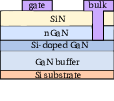
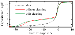

We apply the Terman method to the devices without the AlGaN barrier introduced in Section 2.1. The gate contact is realized on top of the dielectric layer, while the bulk is connected to the silicon doped layer buried into the GaN buffer, as shown in the cross
section in Fig. 3.4a. We use two wafers, one of which has had an additional cleaning (a standard wet chemistry process)
at the GaN surface before the deposition of the dielectric. Their high frequency capacitance characteristic are shown in Fig. 3.4b. The shape of the curve in depletion between −30 V and −20 V is due to the non uniform doping
profile. In fact, at negative gate bias the depletion region grows in the semiconductor, and the depletion depth is proportional to the doping profile. The steeper part of the CV corresponds to the 1018/cm3 Si doped layer, the rest to the
UID GaN (dopant concentration 1016/cm3). This fact also explains the discrepancy between the measured curves and the ideal one, simulated using  1016/cm3. We note that
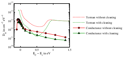
the CV of the structures with the additional cleaning is slightly steeper than the other one, which would imply a smaller amount of trapped charge. The results of the Terman analysis are shown in Fig. 3.5. We obtain a “U” shaped distribution close to the conduction band edge, with an average density of
1013/(cm2 eV). The AlGaN surface cleaning appears to reduce the density of the traps around 0.5 eV of about one order of magnitude.
1016/cm3. We note that
the CV of the structures with the additional cleaning is slightly steeper than the other one, which would imply a smaller amount of trapped charge. The results of the Terman analysis are shown in Fig. 3.5. We obtain a “U” shaped distribution close to the conduction band edge, with an average density of
1013/(cm2 eV). The AlGaN surface cleaning appears to reduce the density of the traps around 0.5 eV of about one order of magnitude.

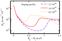
The first limitation of the Terman method is its dependence on parameters, namely the doping profile and the dielectric capacitance. The derivation of Eq. (3.18), which allows us to estimate , assumes a uniform doping profile. It has been
shown that an incorrect value may cause an error of one order of magnitude
in determining the density of interface states [66]. From Fig. 3.6a, we can see that also the shape of the curve is affected. The same happens for the
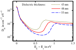
dielectric capacitance, for which the exact dielectric thickness has to be estimated or measured. In our case, the measured value of  is 48 nm, while the nominal value is
50 nm. Discrepancies due to the SiN layer irregularities may result in the underestimation or overestimation of the , as shown in Fig. 3.6b for a variation of 5 nm from the correct value.
is 48 nm, while the nominal value is
50 nm. Discrepancies due to the SiN layer irregularities may result in the underestimation or overestimation of the , as shown in Fig. 3.6b for a variation of 5 nm from the correct value.

A further, more serious limitation is the high frequency approximation. As we explained in the derivation of Eq. (3.18), we assume that the frequency used for the sweep is so high that no traps can follow the AC signal. This allows us to compare the measurement directly with the ideal curve. However, experimental evidence has shown that this interface presents traps with very small time constants, i.e., smaller than 100 ns [47]. It is clear that the high frequency approximation is not valid for these structures. Such a requirement might be met only at frequencies higher than 10 MHz, which would require a dedicated setup with RF probes. Nevertheless, the lower limit for the trapping time constant has not been measured, therefore even higher frequencies might be required.
In addition, this method is based on the assumption the Shockley–Read–Hall model through Eq. (3.4), which means that the traps accessible at a certain DC bias are capturing and emitting back all electrons
following the AC signal. This would be true if the capture and emission time constants were identical for every defect state, namely  . In fact, if we describe
this trapping behavior with a capture–emission time (CET) map, in which the amount of device degradation is plotted as a function of
. In fact, if we describe
this trapping behavior with a capture–emission time (CET) map, in which the amount of device degradation is plotted as a function of  and
and  , we would obtain a narrow stripe along the
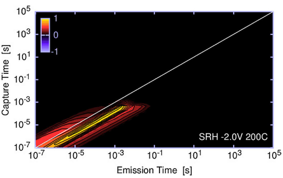
diagonal, and zero otherwise [27], as shown in Fig. 3.7a. On the contrary, the CET map for GaN–based devices shows that there
are interface states with very different capture and emission time constants [47](see Fig. 3.7b). This means that some traps can
capture an electron during the rising part of the AC signal (
, we would obtain a narrow stripe along the
diagonal, and zero otherwise [27], as shown in Fig. 3.7a. On the contrary, the CET map for GaN–based devices shows that there
are interface states with very different capture and emission time constants [47](see Fig. 3.7b). This means that some traps can
capture an electron during the rising part of the AC signal ( ), but they cannot emit it when the gate bias
reaches again the baseline (). For this reason, the assumption of Eq. (3.4) is not adequate for our case.
), but they cannot emit it when the gate bias
reaches again the baseline (). For this reason, the assumption of Eq. (3.4) is not adequate for our case.
The last and most important problem of the Terman method is that it cannot be applied to composite GaN/AlGaN structures. As we mentioned in Chapter 1, the presence of the AlGaN layer results in a small–signal behavior that cannot be modelled with the equivalent circuit described in Section 3.1. We will discuss in detail the role of the AlGaN barrier in Section 3.2.1, showing that the model of Fig. 3.1b should be fundamentally modified. It has been shown that the experimental CV curve can be simulated with a high degree of accuracy just by assuming the modified model, without additional interface traps [46]. Since one of the most important assumptions of the Terman method is not met, this method would lead to erroneous conclusions if applied to GaN/AlGaN MIS structures.

3.1.3 The conductance method
In Section 3.1.1 we derived the expression Eq. (3.12) for the parallel
conductance, , in the case of traps with a single energy  . It is possible to generalize it for an ensemble of
traps distributed in energy, which is a better model of a real system. The integration is possible if we assume the density of traps and the capture probability, which can depend on the surface potential as
. It is possible to generalize it for an ensemble of
traps distributed in energy, which is a better model of a real system. The integration is possible if we assume the density of traps and the capture probability, which can depend on the surface potential as  and
and  , to vary smoothly in a range of few
 . This means that we consider and constant over a small variation of the surface potential. For
this reason, the resolution in energy for will be limited. With this assumption we can
derive the equation [63]
. This means that we consider and constant over a small variation of the surface potential. For
this reason, the resolution in energy for will be limited. With this assumption we can
derive the equation [63]

The quantities  and are extracted with a fit to the experimental
curves, and the density of traps is then calculated with Eq. (3.18).
and are extracted with a fit to the experimental
curves, and the density of traps is then calculated with Eq. (3.18).
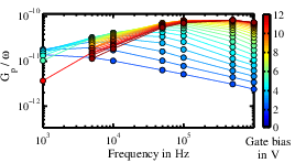
We calculate the parallel conductance from the measured data, and , with the equation

which gives symmetric  peaks as a function of frequency, as
shown in Fig. 3.8. At every gate bias we obtain a different peak, whose maximum value is proportional to the density of
interface states and its resonant frequency is proportional to .
peaks as a function of frequency, as
shown in Fig. 3.8. At every gate bias we obtain a different peak, whose maximum value is proportional to the density of
interface states and its resonant frequency is proportional to .
Similarly to the Terman method, we need to associate at each DC bias the energy of the trap which is in resonance with the AC signal, i.e., the one which is aligned with the Fermi level (see Fig. 3.3). The result of the conductance analysis on the GaN/SiN devices is shown in Fig. 3.9. We obtain the same order of magnitude of traps as with the Terman method, but a slightly different shape at energies
around 1 eV. The device with the additional cleaning process shows a reduced trap density, although the difference is not as marked as in the previous results. In addition, this technique reveals a drop of at energies below −0.1 eV. Negative
energies refer to trap states in the dielectric bandgap and above the semiconductor conduction band edge.
Differently from the Terman method, the conductance technique does not depend in the same way on the parameters used. The only parameter in Eq. (3.22) is the dielectric capacitance, which does not have a strong impact on the calculated peaks. In Fig. 3.10 we compare the results by using the measured dielectric thickness and variations of 5 nm, as we did in Fig. 3.6b. The difference in the result is less than the 6%, and this would not affect the extraction.
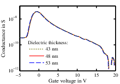
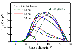

Figure 3.10: The value of the dielectric capacitance used in Eq. (3.22)
does not have such a strong effect as for the Terman method. We obtain the same parallel conductance data at 10 kHz (a) and the peaks at all frequencies (b) using varia-
tions of the dielectric thickness of 5 nm from the measured value.
However, in conductance measurements we should consider the impact of the series resistance. In fact, we can expect that our impedance measurement model is not fully described by a parallel circuit of and , but that also a certain resistance  in series is necessary, especially at high frequency.
This accounts for leakage currents through the dielectric, and for the possible resistance arising from the bulk contact through the Si–doped layer. This can be seen in the measured curves from their behavior at positive bias: the
conductance peak over is not symmetric, but a larger value of
conductance is reached, as shown in Fig. 3.11a. This is the typical effect of the series resistance [38], and can be corrected
with the equations
in series is necessary, especially at high frequency.
This accounts for leakage currents through the dielectric, and for the possible resistance arising from the bulk contact through the Si–doped layer. This can be seen in the measured curves from their behavior at positive bias: the
conductance peak over is not symmetric, but a larger value of
conductance is reached, as shown in Fig. 3.11a. This is the typical effect of the series resistance [38], and can be corrected
with the equations

where the series resistance is evaluated with the high frequency
approximation in accumulation conditions, where the response of the device is assumed to be described by the dielectric capacitance and the series resistance in series. On the contrary, the capacitance curves are not so severely affected. As a result of the
correction with the appropriate value, the peaks become symmetric. If the wrong
series resistance is used, the shape of the curves can be very different. As one can see from Fig. 3.11b, this is true especially
at high frequency, where the impact of the series resistance is larger. Such an artifact compromises the calculation of , because the fit of the peaks with Eq. (3.21) would not converge in this case.
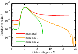
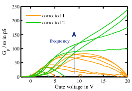

Figure 3.11: The effect of the series resistance parameter in the correction of the parallel conductance data at 10 kHz (a) and of the peaks at all frequencies (b). The first cor-
rection (labeled “corrected 1”) is made with the correct parameter, the second (“corrected 2”) with a value 15% off the real one.
The conductance method suffers from the same limitation of the Terman method when applied to composite GaN/AlGaN structures. As we pointed out at the beginning of the present chapter, the foundations of this technique lie in the equivalent circuit model of Section 3.1.1. The presence of the AlGaN barrier causes the failure of such an assumption, as we will discuss in Section 3.2.1. For this reason, also this method is not adequate for GaN/AlGaN devices.
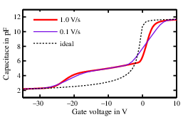
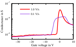

Finally, a problem common to both methods consists in the dependence of the impedance characteristics on the measurement parameters, which will be discussed in detail in Section 3.2.2. In fact, we find that the CV and conductance curves at the same
frequency can vary if the sweep rate is changed. An example is shown in Fig. 3.12. A slow sweep results in a stretch–out of the
CV and a broader conductance peak. It is clear that the results from the Terman and the conductance method would be very different using the slow or the fast data. Moreover, such a behavior contradicts the assumption of thermal equilibrium. In other words,
the trap states are not in resonance with the AC signal, capturing and emitting electrons following the small–signal oscillations, but the DC bias itself causes a time–dependent right shift of the threshold voltage. As a consequence, we cannot define the “baseline”
of the surface potential  and assume that the only change in time,
 , is due to the small–signal
variation of the gate voltage. Therefore, the measurements at various speed give very different
results because the amount of trapped charge depends on the duration of the transients at each gate bias, which is longer the slower the sweep rate. The failure of this fundamental assumption causes the methods described in this section to give very questionable
results even on GaN/SiN MIS structures. We must therefore conclude that the Terman and the conductance method are inappropriate for the characterization of interface traps in GaN–based devices, especially for composite GaN/AlGaN samples.
, is due to the small–signal
variation of the gate voltage. Therefore, the measurements at various speed give very different
results because the amount of trapped charge depends on the duration of the transients at each gate bias, which is longer the slower the sweep rate. The failure of this fundamental assumption causes the methods described in this section to give very questionable
results even on GaN/SiN MIS structures. We must therefore conclude that the Terman and the conductance method are inappropriate for the characterization of interface traps in GaN–based devices, especially for composite GaN/AlGaN samples.
Previous: 2.4 Setup for opto-electrical characterization Top: Home Next: 3.2 Impedance characteristics of GaN/AlGaN MIS structures