« PreviousUpNext »Contents
Previous: 5.2 Results on devices with fluorinated interfaces Top: Home Next: 6.2 Effect of light on MIS structures
6 Opto–electrical characterization of defects
Optical characterization methods allow us to access defects with very large activation energies, which would not be possible to characterize with electrical techniques only. During the course of this thesis the setup for combined optical and electrical characterization, described in Section 2.4, has been established. In this chapter, we present the theoretical foundations for the deep level optical spectroscopy (DLOS) experiment. We apply this method first to GaN/AlGaN samples for the characterization of impurities in the GaN buffer. Then, we investigate the effect of monochromatic light on MIS structures and on MIS–HEMTs, focusing on a method to distinguish defects at the AlGaN/dielectric interface from bulk states. We highlight the challenges of our standard test structures, arising mainly from the light absorption properties of the thick aluminum gate contact. Finally, we introduce new devices designed explicitly for optical investigations, featuring an evaporated gold (or gold and titanium) gate contact as thin as 5 nm, and the first results of DLOS characterization.
6.1 Effect of light on GaN/AlGaN test structures
In this first section we briefly summarize the main principles of optical transitions in charge exchange mechanisms, and we present the concept of the DLOS method. We describe the experimental approach and we analyze the data measured on simple GaN/AlGaN samples, in order to characterize the buffer defects responsible for vertical breakdown.
6.1.1 The DLOS experiment
When a semiconductor device is exposed to light, the photons of the optical radiation can interact with the electrons in the solid material. The motion of the electrons can be described by the hamiltonian 

where the vector potential of the electromagnetic field for monochromatic radiation is

In the electric dipole approximation, we take the first order expansion of the exponential, therefore the hamiltonian Eq. (6.1) becomes simply

Electron emission from a trap can be modelled as the transition of the electron from a bound state (trapped, described by  ) to a state in the conduction band (described
by
) to a state in the conduction band (described
by  ), as introduced in Section 1.2.2. Applying
time dependent perturbation theory, the probability that the electron moves from the trapped to the band state is given by the Fermi golden rule
), as introduced in Section 1.2.2. Applying
time dependent perturbation theory, the probability that the electron moves from the trapped to the band state is given by the Fermi golden rule

We introduce the optical cross section, which is defined as

We note that the photon flux,  , is proportional to the square modulus of
the vector potential (
, is proportional to the square modulus of
the vector potential ( ). In this way, the optical cross section does not depend on
  :
:

Following the derivation of G. Lucovsky [99], we can make some assumptions in order to simplify Eq. (6.6). First, the
matrix elements  can be evaluated starting from the initial and
final wavefunctions and . In the case of a defect located inside the
semiconductor material, we can describe the bound state with a wavefunction of the kind
can be evaluated starting from the initial and
final wavefunctions and . In the case of a defect located inside the
semiconductor material, we can describe the bound state with a wavefunction of the kind

with  , that can
be derived from the assumption of a delta function potential. Furthermore, we can use the parabolic approximation to express the density of states
, that can
be derived from the assumption of a delta function potential. Furthermore, we can use the parabolic approximation to express the density of states  :
:

This assumption is valid around the minimum of the conduction band edge, and for photon energies that do not largely exceed  , the optical activation energy of the
defect. The Lucovsky model for the optical cross section therefore reduces Eq. (6.6) to
, the optical activation energy of the
defect. The Lucovsky model for the optical cross section therefore reduces Eq. (6.6) to

This model can be applied in the analysis of experimental data measured during exposure to monochromatic light. We consider the recovery transient of current (or capacitance) after a certain stress has been applied to the device. Under stress conditions the traps capture electrons, that are then emitted during recovery. The rate of emission under exposure depends on temperature and on the energy of the optical radiation. We have discussed the characteristic time constant for non–radiative transitions in the previous chapters. The rate of emission due to optical radiation is instead

which gives rise to exponential transients of the kind

For this reason, as a first approximation, the initial slope of the transient, normalized to the photon flux, is proportional to the optical cross section. From a series of measurements at various values of photon energies, we can therefore extract the optical cross
section as a function of energy. This approach is very similar to the deep level transient spectroscopy, with the difference that the temperature is kept as low as possible to minimize thermal emission, and the parameter to be varied is the photon energy. For this
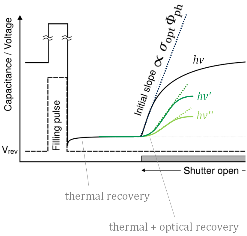
reason, it has been named deep level optical spectroscopy (DLOS) [33, 101]. The experimental procedure is illustrated in Fig. 6.1. As shown
in the figure, a solution to minimize the impact of thermal emission is to wait a short time before turning on the light, so that the trap states with small thermal activation energy emit all their electrons already in dark conditions. At this point, only the states with
larger optical activation energy contribute to the recovery transient measured during exposure. The optical cross section can be therefore extracted in an accurate way. At this point, the Lucovsky model of Eq. (6.9) can be used to evaluate the optical activation energy of the trap states, , and consequently to give an
interpretation of the identity or possible origin of the defect.
6.1.2 C and Mg impurities characterized with O–DLTS
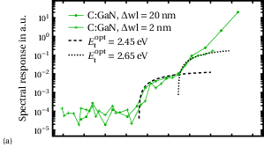
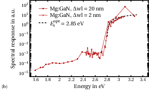
We apply the DLOS method to GaN/AlGaN structures grown on silicon. They have a circular Schottky contact on top, with a diameter of 100 µm that leaves a large area of the AlGaN exposed to the light. We investigate two kind of GaN buffers,
intentionally doped with carbon (with a density of about 1016/cm3) and magnesium (1019/cm3). We bring the devices very close to vertical breakdown, applying about 400 V between the top and
bottom contacts. In this way, it is possible to generate a vertical leakage current by photogeneration, by exposing the structure to monochromatic light. We observe the maximum effect when the photon energy is the same as that of the bandgap, i.e.,
3.39 eV. In addition, we expect to see a “shoulder” to the main peak at energies corresponding to the optical activation energy of the trap states, that contribute to the leakage current by emitting electrons at  . The trap energy
can be extracted with a fit to the data according to Eq. (6.9).
. The trap energy
can be extracted with a fit to the data according to Eq. (6.9).
The spectra of the two investigated samples are shown in Fig. 6.2. We extract the spectral response of the structure under illumination, given in arbitrary units,
which is proportional to the optical cross section. In fact, the normalization obtained by dividing  through the photon flux would be
correct also in absolute values only if the complete light beam was absorbed by the active area of the device. Since its dimensions are much smaller than that of the beam, it is not possible to completely focus the light onto it. As a consequence, only a fraction of
the photons actually illuminates the sample, therefore we can correct our results only for the relative difference of the photon flux within the energy range used. Nevertheless, a fit to the data with the Lucovsky model can give us a good estimate of the optical
energy of the active defects.
through the photon flux would be
correct also in absolute values only if the complete light beam was absorbed by the active area of the device. Since its dimensions are much smaller than that of the beam, it is not possible to completely focus the light onto it. As a consequence, only a fraction of
the photons actually illuminates the sample, therefore we can correct our results only for the relative difference of the photon flux within the energy range used. Nevertheless, a fit to the data with the Lucovsky model can give us a good estimate of the optical
energy of the active defects.
As we can see in Fig. 6.2a, in the carbon–doped sample we can fit two contributions from states with optical activation energy of 2.45 eV and 2.65 eV. Such defects are usually associated to the gallium vacancy in the GaN buffer [34, 35]. The carbon related contribution could be at the upper limit of the energy used for this experiment, as it has been found in other measurements to be around 3.3 eV.
On the other hand, the magnesium–doped sample shows a large shoulder at 2.85 eV, which has in fact been related in literature to the magnesium impurity in GaN [34, 101].
« PreviousUpNext »ContentsPrevious: 5.2 Results on devices with fluorinated interfaces Top: Home Next: 6.2 Effect of light on MIS structures