« PreviousUpNext »Contents
Previous: 3.3 Voltage shift methods Top: Home Next: 4.2 The non-radiative multiphonon (NMP) model
4 Modeling of charge trapping phenomena
Charge trapping phenomena are responsible for the threshold voltage instability of MIS–HEMTs structures under positive gate bias. In the previous chapters, we have focused on the experimental methodologies used to investigate these phenomena. At this point it is necessary to introduce a physical model for the mechanisms of trapping and detrapping. In this chapter we review briefly the Shockley–Read–Hall model and its shortcomings in explaining the experimental data. Subsequently, we give an overview of the non–radiative multiphonon theory that is used as the foundation for our data analysis. We describe the relevant parameters of the model and how to extract them from the data. We perform some simulations in order to highlight advantages and disadvantages of our approach, that will be finally applied to the measurement data on GaN–based devices in Chapter 5.
4.1 The Shockley–Read–Hall (SRH) model
The SRH model was first developed for defects in bulk semiconductors [74, 75], then adapted for interface and oxide traps in MIS (and MISFET) structures by E. H. Nicollian and A. Goetzberger in 1966 [63]. The basic assumption is that the probability
that a carrier at a trap energy  is captured (or emitted) is proportional to its
thermal velocity
is captured (or emitted) is proportional to its
thermal velocity  and a certain cross section
  .
.
Depending on the sign of the carriers in the channel, during operation we have a reservoir of electrons in the semiconductor conduction band (or holes in the valence band) which can charge the traps present in the active energy region (AER). The
AER is that portion of trap states which can change their occupancy state during and after stress. This means that, if the traps in a nMOSFET are donor–like, they are above the Fermi level before stress (unoccupied) and below Fermi level with the application of the
gate bias  (thus trapping an electron). The contrary
happens in the case of acceptor–like states in pMOSFETs. Let’s assume that the defects are located inside the semiconductor bandgap, i.e.,
(thus trapping an electron). The contrary
happens in the case of acceptor–like states in pMOSFETs. Let’s assume that the defects are located inside the semiconductor bandgap, i.e.,  and
and  , where
  is the energy of the electrons at the conduction
band and
is the energy of the electrons at the conduction
band and  at the valence band edge. In this way, there is no
energy barrier for electron capture into donor–like traps (see Fig. 4.1a), and neither for hole capture into acceptor–like states. In this case, the capture rate is expressed simply
by
at the valence band edge. In this way, there is no
energy barrier for electron capture into donor–like traps (see Fig. 4.1a), and neither for hole capture into acceptor–like states. In this case, the capture rate is expressed simply
by

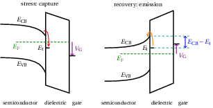

Figure 4.1: Band diagram of a n–type MIS structure during stress (a) and recovery (b). According to the SRH model, there is no energy barrier for electron capture (indicated by the red arrow on the left). On the contrary, for electron emission (orange arrow
on the right) the additional energy  must be provided to the system.
If no further assumptions on are made, the trapping process will be temperature independent. In this way, the temporal
evolution during stress has a single time constant  at all temperatures,
irrespective of the distribution of trap levels throughout the bandgap.
at all temperatures,
irrespective of the distribution of trap levels throughout the bandgap.
On the other hand, under recovery conditions the electron trapped in a donor–like trap can be emitted again, if the Fermi level falls below . Similarly, holes captured in an acceptor–like trap
are emitted if the Fermi level rises above . The rate of emission differs from that of capture
by a Boltzmann factor, depending on the difference of energy between the conduction band edge and the trap level for electrons (see Fig. 4.1b), and  for holes, following the
equations
for holes, following the
equations

The experimental data generally depends on the temperature during both stress and recovery. From Eq. (4.1), we already note that the
temperature dependence during electron or hole capture can be explained only by assuming a temperature–dependent cross section .
Furthermore, as we already discussed in Section 3.1.2, the SRH model does not explain the complex CET map observed in the case of GaN–based MIS–HEMTs. In fact, in Fig. 3.7b we see states with very small time constants for capture but very long ones for emission, while the SRH model allows only
traps with correlated  and
and  , as shown by the result of a simulation in
Fig. 3.7.
, as shown by the result of a simulation in
Fig. 3.7.
We must conclude that this model is inadequate to fully describe charge trapping at the semiconductor/dielectric interface, and therefore we must adopt a different physical model for charge exchange.
« PreviousUpNext »ContentsPrevious: 3.3 Voltage shift methods Top: Home Next: 4.2 The non-radiative multiphonon (NMP) model