« PreviousUpNext »Contents
Previous: 3.2 Impedance characteristics of GaN/AlGaN MIS structures Top: 3 Methodologies for electrical characterization of interface defects in GaN-based MIS-HEMTs Next: 4 Modeling of charge trapping phenomena
3.3 Voltage shift methods
In this section we present two methods to evaluate the voltage shift during positive gate bias stress of a MIS–HEMT device. We rely on impedance measurements in order to be sensitive to the voltage drift in the spill–over region, where the second increase of capacitance and the second conductance peak are observed. However, our aim is to investigate the voltage shift due to the applied DC gate bias during a stress transient. Capacitance measurements have been used in a similar way to investigate the bias temperature instability (BTI) of silicon devices [68]. First, we describe an approach based on the comparison of the CV characteristic before and after stress, the measurement–stress–measurement (MSM) method. Secondly, we propose an “on the fly” method that enables us to evaluate the voltage shift directly during the stress transient, the capacitance–on the fly (C–OTF) method.
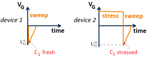
3.3.1 The measurement–stress–measurement (MSM) method
In the previous section, we have shown that the impact of the sweep for characterizing the device can have a larger impact than the actual stress transient. For example, a longer time at negative bias reduces the extracted  , since
  constitutes a recovery condition from a
forward bias stress. For this reason, we apply a method that allows the comparison between fresh and stressed conditions without taking the impedance characteristic over the whole voltage range. Instead, we optimize the starting voltage, indicated as
constitutes a recovery condition from a
forward bias stress. For this reason, we apply a method that allows the comparison between fresh and stressed conditions without taking the impedance characteristic over the whole voltage range. Instead, we optimize the starting voltage, indicated as  , to a value included in the
  region, where the capacitance has the steepest
increase and therefore the sensitivity to the voltage shift is maximized. This approach is therefore a measurement–stress–measurement (MSM) method [69, 70], already extensively used in the study of voltage drifts in silicon, silicon carbide as
well as in gallium nitride transistors [47, 71, 72]. A schematic illustration of the MSM method is shown in Fig. 3.20.
region, where the capacitance has the steepest
increase and therefore the sensitivity to the voltage shift is maximized. This approach is therefore a measurement–stress–measurement (MSM) method [69, 70], already extensively used in the study of voltage drifts in silicon, silicon carbide as
well as in gallium nitride transistors [47, 71, 72]. A schematic illustration of the MSM method is shown in Fig. 3.20.
It is clear that a value close to the threshold voltage is still a
recovery condition for the device, compared with the stress transient at positive gate bias. This is the main drawback of this method, which consists in the inevitable underestimation of the because of the intermediate recovery at the read–out voltage . However, by optimizing the starting voltage and
reducing the measurement delay we can find a trade–off between the accuracy in extracting the voltage shift and the underestimation error.
We investigate the impact of the measurement delay using the lock–in amplifier. In this way we can achieve a delay as short as 1 ms, and we compare the result with a second measurement with delay 250 ms, that is the typical value for a
standard impedance analyzer setup. As we can see from Fig. 3.21a, a longer waiting time at negative bias results in a smaller value of . In the case considered here, this effect can influence the result up to 10% for the
MIS–HEMTs with standard interface.
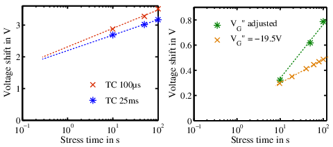

Figure 3.21: Application of the MSM method to MIS–HEMTs with a standard interface. We study the impact of the measurement delay (a), from the smallest value possible with the lock–in amplifier, 1 ms, to the typical delay of an impedance
analyzer, 250 ms. Furthermore, we investigate the effect of using always the same  −19.5 V, instead of optimizing
  as described in the text (b). The dashed lines are
just a guide to the eye.
as described in the text (b). The dashed lines are
just a guide to the eye.
Furthermore, we must take into account that the threshold voltage shifts during stress. It is not uncommon to reach several volts of shift, therefore we might miss the region when we use the same before and after stress. As a consequence, it is
necessary to optimize the starting voltage for the measurement after stress, especially after a long one, to a value which is ideally equal to  . As the voltage shift is not known a
priori, preliminary measurements might be required to determine the best starting voltage for a certain stress. Fig. 3.21b shows the impact of using always the same instead of choosing the proper value of . Since the sweep direction is positive, eventually
we measure the desired region, but the time spent at negative bias before
reaching it has the same effect as a long time delay. The consequence is an additional underestimation of the voltage shift, which is more severe the longer the stress duration. For this reason, the slope of the curve as a function of the stress time is affected.
. As the voltage shift is not known a
priori, preliminary measurements might be required to determine the best starting voltage for a certain stress. Fig. 3.21b shows the impact of using always the same instead of choosing the proper value of . Since the sweep direction is positive, eventually
we measure the desired region, but the time spent at negative bias before
reaching it has the same effect as a long time delay. The consequence is an additional underestimation of the voltage shift, which is more severe the longer the stress duration. For this reason, the slope of the curve as a function of the stress time is affected.
In conclusion, the MSM method allows an accurate extraction of the voltage shift when all the relevant measurement parameters are optimized. Nevertheless, we must be aware of the fact that the extracted is always underestimated.
An additional, important observation regarding the application of this method at different temperatures can be made at this point. As we will see in the next chapters, the temperature dependence of the device degradation is a key factor in understanding the
physical mechanisms responsible for it. We are therefore interested in comparing the voltage drift data at various temperatures. However, both trapping and detrapping events generally depend strongly on temperature. Given the experimental restrictions, an
MSM test would typically be carried out at a constant temperature. The stress transient and the recovery during the read–out phase will therefore have the same temperature, unless special devices for fast temperature switching were used. For example, this has
been possible for silicon devices by means of the poly heater, a structure of two polycrystalline silicon wires in close contact with the device under test, that allows swift temperature changes [73]. If the temperature is the same during stress and recovery, the MSM
method suffers from additional drawbacks. In the first place, the shape of the CV curve depends on temperature, therefore also the proper values of and of are temperature dependent. These values must
be carefully evaluated in order to make the direct comparison of measurement at different temperatures possible. Moreover, the effect of the recovery during the time delay would also be temperature dependent. This means that the underestimation error in the
extracted changes with temperature as well. As a consequence, it is very challenging to determine
the real dependence of the device degradation on temperature. A solution can be found by separating the trapping and detrapping events, by focusing on the stress transients only. This is the basic concept of the method presented in the next paragraph.
3.3.2 The capacitance–on-the-fly (C–OTF) method
The idea of an “on the fly” method is to evaluate the device degradation directly during the application of a stress voltage. This kind of approach has been developed for current–voltage experiments to investigate the BTI on silicon MOSFETs [69, 70]. In
our case, the drain current transient of a GaN/AlGaN MIS–HEMT at positive bias would not allow us to accurately extract the voltage shift, because the current is close to the saturation value in this region of operation. On the contrary, the CV curve shows the
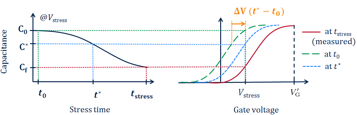
second increase of capacitance when spill–over is reached, providing a high sensitivity to voltage shifts. By choosing a stress voltage  in spill–over conditions, we can interpret the
decreasing capacitance transient as a right shift of the whole capacitance characteristic. This can be done by comparing the capacitance value during stress with that of a reference CV curve, which is measured after the stress transient, as shown in Fig. 3.22. From the shift we can then calculate the density of active interface traps
in spill–over conditions, we can interpret the
decreasing capacitance transient as a right shift of the whole capacitance characteristic. This can be done by comparing the capacitance value during stress with that of a reference CV curve, which is measured after the stress transient, as shown in Fig. 3.22. From the shift we can then calculate the density of active interface traps  with Eq. (1.1).
Since the characteristic is taken after stress, the capacitance  corresponding to in the CV curve is the value at the last
measurement point of the transient, at
corresponding to in the CV curve is the value at the last
measurement point of the transient, at  . Instead, the capacitance
  at the first measurement point,
  , gives the position of the CV curve of the fresh device, as
shown in Fig. 3.23 with the long dashed line. In a similar way, for every time
, gives the position of the CV curve of the fresh device, as
shown in Fig. 3.23 with the long dashed line. In a similar way, for every time  between and we can find the intermediate CV curve
position, indicated by the short dashed line in the illustration. At this point, is calculated as the horizontal shift between the CV curve at and that at . Repeating this procedure for every data point of the
transient we extract the time evolution of the device shift.
between and we can find the intermediate CV curve
position, indicated by the short dashed line in the illustration. At this point, is calculated as the horizontal shift between the CV curve at and that at . Repeating this procedure for every data point of the
transient we extract the time evolution of the device shift.
Obviously, the modalities of the CV reference measurement are of primary importance. We study in the first place the impact of the sweep direction. As we discussed previously in Section 3.2.2, at positive gate voltages a negative sweep direction allows the
effect of electron capture and emission to partially balance each other out. This results in the CV curve having the least contribution of trapping during the sweep itself. For this reason, we choose to perform the reference CV curve measurement starting from a
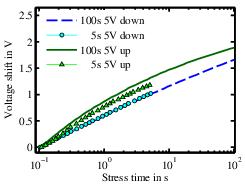
positive voltage, , going then down to zero. A clear argument in
favor of this choice is the comparison of the temporal evolution of over two different values of stress duration, 5 s and 100 s. We expect our
method to give consistent results in the portion of stress time in common with the two measurements. As we can see from Fig. 3.24, when we use a negative sweep direction (“down”) our expectation is
met. On the contrary, the positive (“up”) sweep leads to a contradictory result. This is due to the fact that additional electron trapping takes place during the CV measurement, thus distorting the capacitance characteristic. As a consequence, the time evolution has a different shape for the two stress durations.
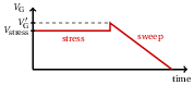
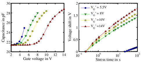
The starting voltage of the CV sweep is also very important. As we can see from Fig. 3.23, the value of must be larger than in order to allow for the calculation of the
voltage shift. However, we have proven in Section 3.2.2 that a too large value might influence the shape of the CV curve to the point that the impact of sweeping dominates on that of the stress. The ideal starting voltage is in fact  . For this reason, we must
optimize it for every stress duration. We investigate the impact of varying for a stress of 5 V for 100 s. We
use values slightly or much larger than , namely 5.5 V up to 14 V.
The results are shown in Fig. 3.25. When the starting bias is much higher than stress, the additional trapping events during the sweep cause the distortion of the CV curve, that in turn results in an
overestimated for long stress times. The larger , the larger the error on the slope of as a function of time. The error in this example is up to 20% at
. For this reason, we must
optimize it for every stress duration. We investigate the impact of varying for a stress of 5 V for 100 s. We
use values slightly or much larger than , namely 5.5 V up to 14 V.
The results are shown in Fig. 3.25. When the starting bias is much higher than stress, the additional trapping events during the sweep cause the distortion of the CV curve, that in turn results in an
overestimated for long stress times. The larger , the larger the error on the slope of as a function of time. The error in this example is up to 20% at  100 s. On the contrary, a too small
difference between and does not allow to extract the voltage shift for the
first part of the transient, as can be seen when we use 5.5 V. As a consequence, a trade–off must
be found. We must determine the voltage value that allows to extract the voltage shift for short stress time, while avoiding an excessive additional stress. This problem must be properly addressed in particular when the stress duration is very long, or for very small
measurement delays. In fact, even if the first measurement point of an experiment with the lock–in amplifier is at
100 s. On the contrary, a too small
difference between and does not allow to extract the voltage shift for the
first part of the transient, as can be seen when we use 5.5 V. As a consequence, a trade–off must
be found. We must determine the voltage value that allows to extract the voltage shift for short stress time, while avoiding an excessive additional stress. This problem must be properly addressed in particular when the stress duration is very long, or for very small
measurement delays. In fact, even if the first measurement point of an experiment with the lock–in amplifier is at  50 µs, the extraction of is not possible until about 10 ms. The data in Fig. 3.25 is measured with the impedance analyzer, which has a time delay of 250 ms. This is the reason why the first point does not decrease at larger . In this way the difference in slope is clearer in
the figure.
50 µs, the extraction of is not possible until about 10 ms. The data in Fig. 3.25 is measured with the impedance analyzer, which has a time delay of 250 ms. This is the reason why the first point does not decrease at larger . In this way the difference in slope is clearer in
the figure.

We can distinguish three approximations made in the C–OTF method that limit its accuracy. In the first place, we assume a parallel shift of the CV curve as a whole during stress at positive bias. This might be imprecise for very long stress duration at large stress
bias, or when a too large is chosen. The second approximation is to
neglect the additional stress induced by a larger than the stress voltage. This effect
contributes to the overestimation of the . Finally, the third limitation is the impossibility to determine the amount of voltage shift at
the first measurement point,  . In fact, we must assume that the CV curve of the
device in fresh conditions is the one extracted from the first measurement point. However, the real value of capacitance right after stress is impossible to measure, because of the inevitable time delay of the instrument. In all time–resolved measurements we
always observed a decreasing behavior, which means that the trapping phenomena causing the drift start playing their role before our time resolution of 50 µs. As a consequence, we arbitrarily set the unknown of all C–OTF measurements to zero.
. In fact, we must assume that the CV curve of the
device in fresh conditions is the one extracted from the first measurement point. However, the real value of capacitance right after stress is impossible to measure, because of the inevitable time delay of the instrument. In all time–resolved measurements we
always observed a decreasing behavior, which means that the trapping phenomena causing the drift start playing their role before our time resolution of 50 µs. As a consequence, we arbitrarily set the unknown of all C–OTF measurements to zero.
In conclusion, the C–OTF method allows us to evaluate the device degradation over time, extracting the voltage shift directly from the data measured during stress. The error due to the approximations used can be limited by choosing the proper parameters for the measurement of the CV characteristic, except for the inevitable effect of the experimental time delay, as for the MSM approach. In Chapter 5 we show a direct comparison of the two methodologies described in this Section (MSM and C–OTF) on different GaN–based samples. Furthermore, the C–OTF method enables the direct comparison of the results taken at different temperatures. In the next Chapter 4 we introduce some fundamentals about the modeling of the degradation mechanisms, that are then applied in Chapter 5 on C–OTF measurements on our test structures.
« PreviousUpNext »Contents
Previous: 3.2 Impedance characteristics of GaN/AlGaN MIS structures Top: 3 Methodologies for electrical characterization of interface defects in GaN-based MIS-HEMTs Next: 4 Modeling of charge trapping phenomena