« PreviousUpNext »Contents
Previous: 5 Electrical characterization of interface defects in GaN-based MIS-HEMTs Top: 5 Electrical characterization of interface defects in GaN-based MIS-HEMTs Next: 6 Opto-electrical characterization of defects
5.2 Results on devices with fluorinated interfaces
The fluorination of the AlGaN surface before the deposition of the dielectric results in particular device properties, which are observed only when this cleaning process is used. The differences to the standard devices indicate that fluorine plays an active role in passivating the native surface donor states, while it gives rise to an additional type of defect. In this section we describe the characteristics of the fluorinated GaN/AlGaN MIS–HEMTs, investigating their behavior under forward and reverse gate bias conditions. Finally, we evaluate the density of interface traps and compare it with that of standard devices.
5.2.1 Effect of fluorination on device behavior
The fluorination process at the AlGaN/SiN interface results in a slightly reduced 2DEG density of the MIS–HEMT devices, namely 5.5 × 10¹²/cm2 instead of 7.3 × 10¹²/cm2 [54], but, on the other
hand, threshold voltage drifts appear to be consistently reduced and the hysteresis is almost absent, as we can see in Fig. 5.7. Furthermore, there is no increase of
capacitance at positive gate bias. The capacitance takes the value of the plateau,  ,
until breakdown of the device around 20 V.
,
until breakdown of the device around 20 V.
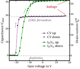
We can explain the absence of the spill–over capacitance by studying the trapping behavior. Electron capture can be measured with our setup only around the threshold voltage, i.e., when the gate bias is switched from a value in depletion to one above  . When a more positive bias is applied, transients
are stable down to microseconds [54]. This means that our experimental setup is too slow to appreciate electron trapping, which takes place entirely before we can measure the first point. For this reason, the devices appear to be always in equilibrium
conditions. If we could measure the CV curve at the time scale of electron capture, we would indeed observe the second rise of capacitance in spill–over conditions. However, the electrons are promptly trapped at interface states and therefore the capacitance
returns again to the plateau value. Since the trapping phenomena cannot be investigated with our time resolution, we focus on the electron emission process instead.
. When a more positive bias is applied, transients
are stable down to microseconds [54]. This means that our experimental setup is too slow to appreciate electron trapping, which takes place entirely before we can measure the first point. For this reason, the devices appear to be always in equilibrium
conditions. If we could measure the CV curve at the time scale of electron capture, we would indeed observe the second rise of capacitance in spill–over conditions. However, the electrons are promptly trapped at interface states and therefore the capacitance
returns again to the plateau value. Since the trapping phenomena cannot be investigated with our time resolution, we focus on the electron emission process instead.
Electron detrapping can be studied by holding the device at a certain positive bias, at which equilibrium conditions are reached before 1 µs, and then switch the voltage to a more negative value. Interestingly, drain current transients are observed at any gate voltage down to depletion. The increase of the current implies a negative shift of the transfer characteristic, as shown in Fig. 5.8a for a hold bias of 10 V and recovery voltages from 10 V to −20 V. For all recovery voltages, the current reaches a saturation value within 1 s. This means that after this time the negative shift has reached its final value, and the device does not drift anymore. As a consequence, the position of the transfer characteristics at subsequent times remains the same, as shown in Fig. 5.8b. This is the reason why we do not observe hysteresis with a standard double–sweep measurement, because it takes usually a few seconds to be performed. In this way, the device appears to be very stable.
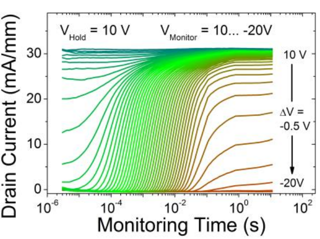
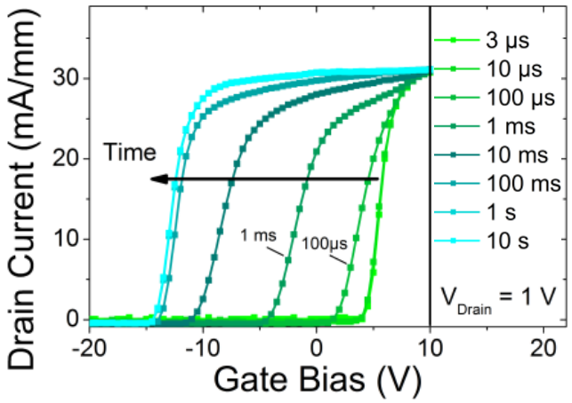

Figure 5.8: Drain current transients (a) when the gate bias is switched from 10 V to a recovery voltage value from 10 V to −20 V. The transfer characteristics (b) are extracted by interpolating the drain current values at various times over all gate voltages. The negative shift saturates after about 10 ms (adapted from [54]).
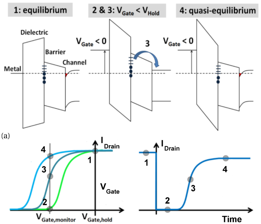
This behavior can be explained with the presence of a very high density of interface states with an energy very close to the Fermi level. The band diagram during stress and recovery is illustrated in Fig. 5.9a: in equilibrium conditions, the traps are filled with electrons, and the drain current has the value 1, indicated in the transfer characteristic in Fig. 5.9b and as a function of time in Fig. 5.9c. When the gate bias is
switched to more negative values, the Fermi level is brought down, the 2DEG is depleted and, consequently, the drain current decreases to the value 2. However, at this point the trapped electrons are emitted back to the 2DEG, resulting in an increase of the drain
current to the value 3 and, eventually, to the value 4, which is almost the same as it was in equilibrium conditions. The increase of the drain current at constant recovery voltage corresponds to a negative shift  , as shown in Fig. 5.9b with the sequence of consecutive transfer characteristics.

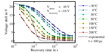
We study the temperature dependence of electron emission with a series of isothermal measurements at our probe station. We hold a stress bias of 10 V for a few seconds and then switch to the recovery voltage of −10 V, monitoring the drain current increase for 1 s. As expected, variations of the stress time from 1 s to 100 s did not affect the result, as the device remains in equilibrium conditions. We span a temperature range from −30 °C to 200 °C by using the thermostatic chuck. The results in terms of voltage shift as a function of time are shown in Fig. 5.10. We note that at higher temperatures the transients accelerates; however, the drain current always comes to the saturation value within 1 s. An exponential curve with a single time constant of 100 µs is also shown in order to compare the shape of the transient. It is clear that the measured curves, although quite fast in reaching saturation, cannot be properly fitted with a single exponential. For this reason, the activation energy would not have a single value but rather a narrow distribution around a mean value. We extract the activation energy spectrum with the Primak method in the next section.
5.2.2 Evaluation of the interface trap density
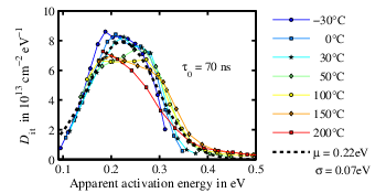
We analyze the dataset of Fig. 5.10 with the Primak method. The result is shown in Fig. 5.11: the value of  obtained with the optimization algorithm is
70 ns, and the
obtained with the optimization algorithm is
70 ns, and the  as a function of activation energy is narrowly
distributed. We can fit the whole dataset with a gaussian function, using a mean value of 0.22 eV and standard deviation of 70 meV. We note that the width of the distribution is larger than the energy resolution of the Primak method, which has
been estimated to be around 25 meV in Section 4.3.2. The density of defects per unit area and energy is 8 × 10¹³/cm2, few times larger than that of devices with the standard interface.
as a function of activation energy is narrowly
distributed. We can fit the whole dataset with a gaussian function, using a mean value of 0.22 eV and standard deviation of 70 meV. We note that the width of the distribution is larger than the energy resolution of the Primak method, which has
been estimated to be around 25 meV in Section 4.3.2. The density of defects per unit area and energy is 8 × 10¹³/cm2, few times larger than that of devices with the standard interface.


However, we can observe that not every part measured at different temperature connects with the others to build a smooth spectrum. This is true for any value of : longer characteristic time constants allow a good
alignment of the measurements at low but not at high temperature, and vice versa for shorter time constants. This is an indication that the approximation of a constant does not hold true in this case. In fact, as we have
seen in Section 4.3.3, the Arrhenius plot extracted from this data (shown in Fig. 4.8) is not linear.
We have discussed few reasons that might explain such a behavior in Chapter 4. One of them is the presence of tunnelling as an additional charge transport mechanism next to NMP transitions, and the consequent failure of the classic approximation. We
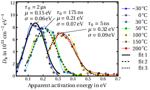
investigate the temperature dependence of  and by repeating the Primak analysis in three separate
groups of temperatures, combining together the three lowest values (-30, 0, 30 °C), the three highest (100, 150, 200 °C) and the remaining three ones in the middle range (30, 50, 100 °C). As shown in Fig. 5.12, the lower the temperature the smaller is the extracted activation energy. This would in principle fit to the model described in Fig. 4.3b. In fact, the impact of tunnelling over that of NMP transitions is larger at low temperatures. Therefore, the error made with the Primak approach, which assumes only NMP
transitions for charge exchange, is larger at low temperatures. In conclusion, according to this hypothesis the best estimate for the activation energy for electron emission is the one extracted at high temperature. In our case, we set the lower limit for to be the one extracted with the fit at high temperature
(labeled “fit 3” in Fig. 5.12). The result is a gaussian distribution with a mean of 0.32 eV and a standard deviation of 90 meV.
and by repeating the Primak analysis in three separate
groups of temperatures, combining together the three lowest values (-30, 0, 30 °C), the three highest (100, 150, 200 °C) and the remaining three ones in the middle range (30, 50, 100 °C). As shown in Fig. 5.12, the lower the temperature the smaller is the extracted activation energy. This would in principle fit to the model described in Fig. 4.3b. In fact, the impact of tunnelling over that of NMP transitions is larger at low temperatures. Therefore, the error made with the Primak approach, which assumes only NMP
transitions for charge exchange, is larger at low temperatures. In conclusion, according to this hypothesis the best estimate for the activation energy for electron emission is the one extracted at high temperature. In our case, we set the lower limit for to be the one extracted with the fit at high temperature
(labeled “fit 3” in Fig. 5.12). The result is a gaussian distribution with a mean of 0.32 eV and a standard deviation of 90 meV.


From all the experimental data and the Primak analysis we can conclude that the fluorination process results in a drastic modification of the defects at the AlGaN/dielectric interface, which makes the device behavior more stable. Since the 2DEG density is
affected [54], fluorine plays a role in the modification of the surface donor states responsible for the creation of the electron gas, at least partially. The new interface state has a narrowly distributed activation energy around a rather low mean value
(0.32 eV) and a large density per unit area and energy (8 × 10¹³/cm2). The small leads to the rather fast detrapping mechanism observed
experimentally, while the is large enough to cause the large voltage shift
described in Fig. 5.9.
Physical–chemical investigations have shown that the fluorine radical F competes with the hydrolytic group OH for the AlGaN surface bonds, giving rise to a highly polarized bond [98]. This increases the
electronegativity of the surface termination, which therefore results in a considerably different AlGaN/SiN interface than in standard devices. The modification impacts both the density and the dynamic response of the interface states. In conclusion, the
fluorination process can be considered a “defect engineering” tool, capable of improving the device performance in terms of reliability.
competes with the hydrolytic group OH for the AlGaN surface bonds, giving rise to a highly polarized bond [98]. This increases the
electronegativity of the surface termination, which therefore results in a considerably different AlGaN/SiN interface than in standard devices. The modification impacts both the density and the dynamic response of the interface states. In conclusion, the
fluorination process can be considered a “defect engineering” tool, capable of improving the device performance in terms of reliability.
« PreviousUpNext »Contents
Previous: 5 Electrical characterization of interface defects in GaN-based MIS-HEMTs Top: 5 Electrical characterization of interface defects in GaN-based MIS-HEMTs Next: 6 Opto-electrical characterization of defects