

Impact of Charge Transitions at Atomic Defect Sites on Electronic Device Performance
Chapter 1 Introduction
Semiconductor-based devices have revolutionized everyday life since the first demonstration of a metal-oxide-semiconductor field-effect transistor (MOSFET) in the late 1950s. The efforts taken by researchers towards ever more powerful and reliable electronics have led to a technology that dominates both the professional and private life of people all around the world. Be it through carrying around access to almost the entirety of human-gathered information in your pockets, by supporting the organization of corporations, banking systems, or even whole countries, or by simply remotely activating your robot vacuum cleaner on the self-driven subway heading home. Invisible to the naked eye, microchips provide humankind with capabilities that were impossible only a few decades ago. Still, for most of us, a world without this enormous computational potential readily at our fingertips has become unimaginable.
A driving force behind the rapid growth of computational power is the constant and ongoing downscaling of the electronic components. This trend is described by the empirical Moore\(^\prime \)s law, stating that the number of electronic components per unit area grows exponentially with the years of development. Although already formulated in 1965, the constant shrinking rate has been observed over decades, propelled by the rapid progression in various areas of research and development. This includes theoretical investigations of the electronic properties of semiconductors and insulators, advances in technology to refine material growth methods, experimenting with various material stacks to optimize the device performance or development of more sophisticated transistor architectures.
As a result, nowadays, transistors with gate lengths in the low nanometer regime can be fabricated. At such small scales, slight deviations from the ideal atomic structure in the materials or their shared interfaces, commonly known as defects, can lead to undesired phenomena which can degrade the performance of electronic devices. For example, defects in the oxide layer and the oxide/channel interface of MOSFETs can trap charges from the substrate during operation [1, 2, 3, 4], which alters the electrostatics of the device and can be the cause of leakage currents [5]. In superconducting qubits, defects in the oxide layer of the Josephson junction (JJ) can introduce two-level system (TLS) that might couple to the qubit state [6], causing decoherence and the avoided level crossing as detected in spectroscopy experiments [7].
On the other hand, defects can also be vital for the functionality of certain electronic devices. For instance, impurities such as phosphorus or boron are deliberately introduced in the Si channel to provoke an excess of electrons or holes in the semiconductor. This process is generally known as \(n\)-type and \(p\)-type doping, respectively, and is crucial to modify the conductivity of many devices. In charge trap flash (CTF) devices, the memory effect originates from charges localized at defective sites in the storage layer [8, 9]. Therefore, silicon nitride is commonly used for this layer due to its high density of charge trapping sites. In some qubit technologies, the defect itself is a crucial component of the device, where the spin state of a charged defect provides a platform for quantum computing [10].
Defects can manifest in various forms, be it as a vacancy, where an atom is missing in the lattice structure, an impurity, where an atom, which is originally not part of the chemical compound, is incorporated in the atomic structure or dangling bonds, where an atom has an unpaired electron due to the absence of a covalent bonding partner. In this thesis, the focus lies on the investigation of charge transitions at various defect sites in oxides and semiconductors and their impact on the performance of electronic devices. Quantum mechanical calculations will be used to analyze the electronic structure of defects and to study the mechanisms behind charge transitions.
1.1 Motivation
The motivation for the main investigations in this thesis are outlined in the following sections.
1.1.1 Hydrogen-related defects in amorphous silicon dioxide (\(a\)-SiO2)
The content presented in this section has been published in [4].
Both the text and the figure have been adapted from this publication.
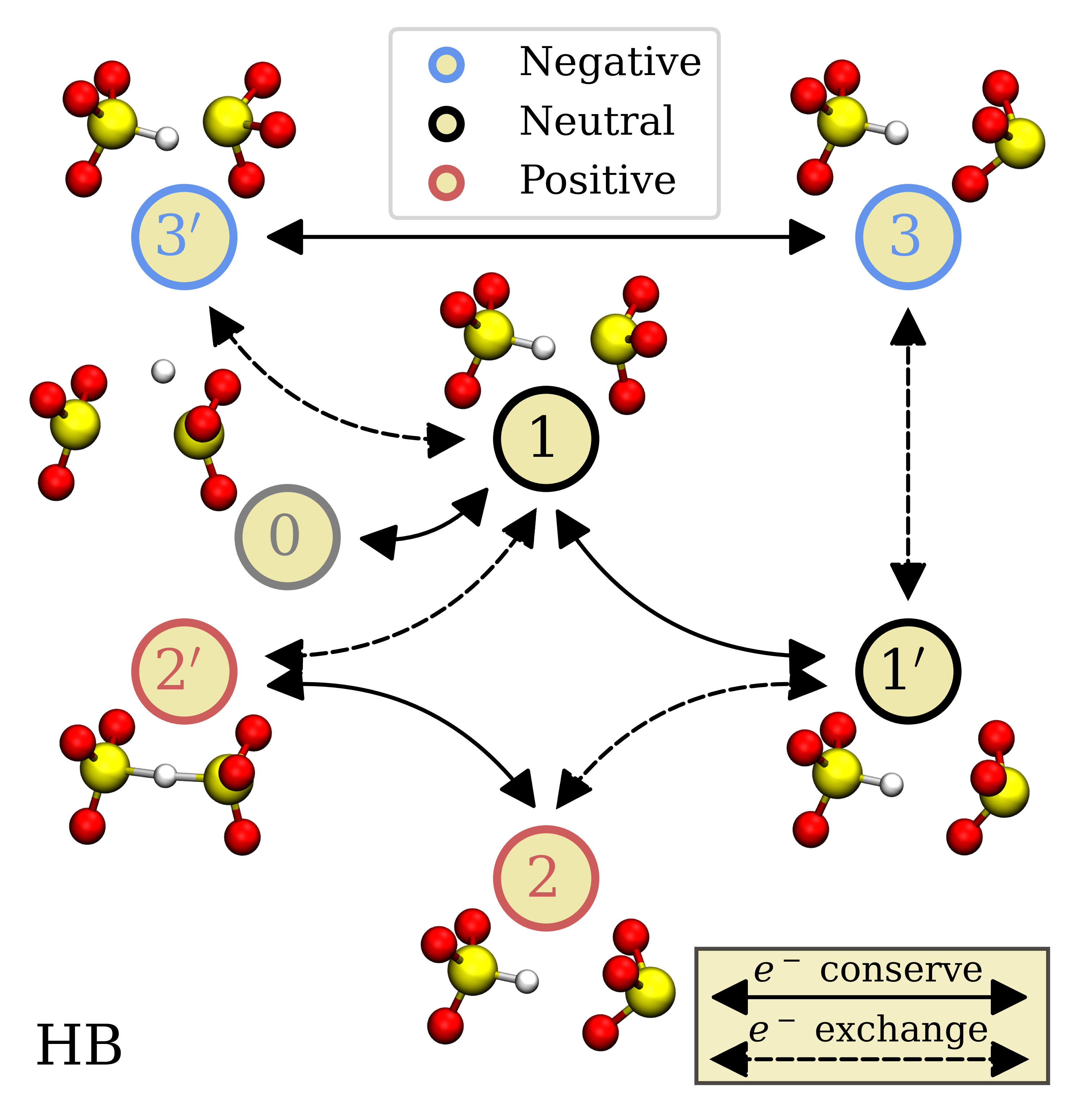
Over the last decades, amorphous silicon dioxide (a-SiO\(_2\)) has played a major role in the fields of optics, electronics and quantum computing, being heavily used in industry as an optical fiber or as the gate oxide of MOSFETs, respectively. Even though charge trapping phenomena at defects in a-SiO\(_2\) have been the focus of many theoretical and experimental studies in the past [11, 12, 13, 14, 15, 16, 17], many open questions concerning the intricate defect dynamics still remain, as investigations in this amorphous material are highly challenging. This is because each single point defect is expected to behave differently, yielding individual defect “footprints”. In particular, it is understood that the same defects can be involved in both hole and electron trapping processes as visualized in the state diagram of a single hydrogen bridge (HB) defect in three charge states in Fig. 1.1, including metastable configurations.
Furthermore, due to transitions between stable and metastable defect configurations in the same charge state, defects may stay electrically inactive for a long time (even months) [18], which highlights the complexity of the involved defect dynamics and requires sophisticated models to be fully understood. Although the classic gate oxide SiO\(_2\) in scaled electronics has been steadily augmented with an additional layer of a high-\(\kappa \) insulator, a thin interfacial layer of SiO\(_2\) has proven to be beneficial for device performance [19, 20, 21]. This is because the interfacial layer ensures good lattice matching with Si and reduces the defect density at the interface [21, 22, 23, 24]. Even in ultra-scaled devices, a thin layer of SiO\(_2\) persists due to the oxidation of the Si surface by excess oxygen atoms during e.g. HfO\(_2\) film growth and due to Si diffusion into the film [25, 22]. Defects in this interfacial layer have a particularly strong impact on the device degradation because of their close proximity to the device channel and therefore often dominate the degradation [2] which motivates further investigations in SiO\(_2\). The hole trapping mechanism in \(a\)-SiO\(_2\) has already been examined at some depth using a four-state defect model [26, 14, 27, 1]. Hereby, the charge transfer reactions were characterized by a nonradiative multi-phonon (NMP) process, while the thermal reconfigurations were described using transition state theory. However, a consistent description including the electron trapping process is still missing.
While the oxygen vacancy [13, 28, 29] is unlikely to change its charge state via interactions with the channel or gate in scaled Si devices due to its low charge trapping level (\(\langle E_\mathrm {T} \rangle - E_\mathrm {V}(\mathrm {Si})\sim 3\) eV) [30, 31, 32], hydrogen related defects in SiO\(_2\) have gained a lot of interest in the recent past in both electronics [26, 33, 34, 35] as well as in optical fibers, where H is known to introduce losses by forming hydroxyl groups in the silica [36, 37]. This is primarily because hydrogen is not only present during many fabrication processes but is also deliberately introduced in semiconductor devices during a forming gas anneal. Such annealing is performed to passivate Si dangling bonds at the interface, which would otherwise drastically reduce the channel mobility and the ON/OFF ration of the device [38, 39, 40, 41]. However, once introduced, hydrogen easily diffuses through the oxide [42, 43, 44] and can trigger detrimental reactions within the amorphous SiO\(_2\) network, creating new defect types suspected to have charge transition levels (CTLs) near the band edges of Si and SiC substrates [26, 45, 46]. For example, H can create point defects in SiO2 like the hydroxyl-\(E^\prime \) center (H-\(E^\prime \)) [47, 48, 33], where a hydrogen attaches to and eventually breaks an already strained Si–O bond, thereby forming a hydroxyl group. Hydrogen can also interact with preexisting defects, e.g. by forming an active hydrogen bridge from an oxygen vacancy [49, 50, 51, 28, 52].
1.1.2 Intrinsic charge trapping sites in amorphous silicon nitride (\(a\)-Si\(_3\)N\(_4\):H)
The content presented in this section has been published in [53, 54, 55].
The text has been adapted from these publications.
Silicon nitrides are widely used as the charge storage layer of non-volatile memory devices such as charge trap flash (CTF) [8, 56], due to their high trap densities (\(\sim \)\(10^{19}\) cm\(^{-3}\) [57, 58]). In CTFs, the charge storage layer is separated from the gate and the substrate by a blocking and a tunneling oxide, respectively, as for example realized in silicon-oxide-nitride-oxide-silicon (SONOS) [8, 59] or TaN/Al\(_2\)O\(_3\)/Si\(_3\)N\(_4\)/SiO\(_2\)/Si (TANOS) [9] technologies. When a positive (negative) voltage is applied to the gate of a CTF, electrons (holes) can tunnel through the tunneling oxide and localize at specific charge trapping centers in the silicon nitride, corresponding to the program (erase) cycle of the memory device [60, 61]. The trapping sites responsible for the storage of charge in Si\(_3\)N\(_4\) are still under discussion.
Dangling bonds have been identified as amphoteric trapping centers by spin resonance experiments and theoretical calculations [62, 63, 64, 65], but exist in too small concentrations (\(\sim \)\(10^{16}\)–\(10^{18}\) cm\(^{-3}\) [65, 66, 58, 67]) to account for the entire charge trapping mechanism in this material. The comparably low concentration of dangling bonds can be attributed to the high H content in these systems, passivating most of the dangling bonds [68], and resulting in large concentrations of Si–H and N–H sites (\(\sim \)\(10^{22}\) cm\(^{-3}\) [69, 70, 71, 72]). However, most of the previous theoretical studies investigating the charge trapping in \(a\)-Si\(_3\)N\(_4\) did not consider realistic H content in the sample structures [63, 73].
This motivates the investigation of intrinsic trapping sites in silicon nitride, as theoretical investigations of electronic states introduced by over- and under-coordinated atoms in Si\(_x\)N\(_y\):H [74] and the localization of electrons in amorphous Si\(_3\)N\(_4\) (\(a\)-Si\(_3\)N\(_4\)) at these sites [63, 75] indicate a variety of possible charge trapping centers in amorphous silicon nitrides. Recently, polarons, which can be described as quasi-particles that form via interactions of charge carriers with lattice vibrations, have been identified as deep acceptor and donor states in different amorphous material systems [76, 15]. Such polaron states might explain the discrepancy between the concentration of dangling bonds and total charge trapping sites. For memory devices employing silicon nitride as the charge trapping layer, it was experimentally shown that H annealing does not have a large impact on the program/erase cycles of these devices, indicating that intrinsic or polaronic sites might dominate the charge trapping mechanism in \(a\)-Si\(_3\)N\(_4\):H [77, 78]. To validate this assumption, this work provides a first-principles description of the charge trapping properties of intrinsic sites in silicon nitride. The localization of holes and electrons at structural defects in \(a\)-Si\(_3\)N\(_4\) will be analyzed as well as polaron formation in hydrogenated silicon nitride (\(a\)-Si\(_3\)N\(_4\):H).
1.1.3 Vacancies in corundum aluminum oxide (\(\alpha \)-Al\(_2\)O\(_3\))
The content presented in this section is currently prepared for publication [79].
Alumina (Al\(_2\)O\(_3\)) is a wide band-gap metal oxide with a broad range of applications in electronic devices. In metal-oxide-semiconductor (MOS) technologies, Al\(_2\)O\(_3\) can be used as a high-\(\kappa \) gate dielectric [80], to passivate the surface of Si substrates [81] or as the tunneling layer of non-volatile flash memory devices [82]. Emerging devices with channels made of 2D materials frequently employ Al\(_2\)O\(_3\) either as an insulator or as a buffer layer to HfO\(_2\) [83, 84]. Moreover, Al\(_2\)O\(_3\) is frequently used in superconducting qubits. The key component in these devices is a JJ, which is commonly realized as an Al/Al\(_2\)O\(_3\)/Al stack [85]. Al\(_2\)O\(_3\) is also an attractive choice for the substrate of superconductor-based integrated circuits due to its exceptionally low dielectric loss value [86, 87, 88].
In all these devices, defects in the oxide layer can lead to reliability issues, as charges from the substrate can localize at the defect sites and consequently change the electrostatics. In MOS devices, this results in changes of important device characteristics such as the threshold voltage. Similarly, the quantum information of a qubit is sensitive to defect states [6] and small quanta such as photons. A possible cause for decoherence [6, 89] and the avoided level crossings seen in qubit spectroscopy [90] are two-level systems (TLS) that couple strongly to the qubit [91]. Defects in the substrates or the tunnel barrier of the Josephson junction have been suspected to be a plausible source of such TLS [92, 89]. Still, the microscopic origin of the TLS is under vivid debate. Thus, to gain a better understanding of decoherence phenomena and to improve the performance of superconducting qubits and MOS devices, a thorough understanding of the structural, electronic and optical properties of potential defect candidates is crucial.
Over the past decades, significant theoretical and experimental efforts have been devoted to analyzing the oxygen vacancy (\(V_\mathrm {O}\)) in Al\(_2\)O\(_3\) [93, 94, 95, 96, 97]. Removal of an oxygen atom from the corundum lattice results in two electrons remaining at the vacancy site in the neutral charge state. Removing one or both of these electrons results in \(V_\mathrm {O}^{+1}\) or \(V_\mathrm {O}^{+2}\) defects. The oxygen vacancy can be classified as a deep donor, as calculations [95] have shown it to have \(0/+1\) and \(+1/+2\) CTLs deep inside the band gap.
In contrast, the aluminum vacancy (\(V_\mathrm {Al}\)) can be classified as a deep acceptor since it can capture up to three additional electrons at the defect site [95, 98]. Theoretical studies have predicted that the most stable configuration of the \(V_\mathrm {Al}\) is a split vacancy (\(V_\mathrm {Al, s}\)) [98, 99, 100, 101]. In this configuration, an Al atom occupies the interstitial site halfway between two Al vacancies along the \(c\)-axis. To date, only the stable charge states and the corresponding CTLs have been reported for vacancies in the corundum structure of alumina (\(\alpha \)-Al\(_2\)O\(_3\)). While the CTLs give a good estimate of the energetic position of optical transitions at the defect site, these levels alone can not account for the vibrational broadening as detected in spectroscopic measurements. The line shape of absorption and luminescence spectra gives information about the structural relaxations upon electronic transitions at the defect site. By considering optical transitions between vibronic levels of defects, it is possible to predict the form of the according line shape and, therefore, to identify optical spectra with distinct electronic transitions at investigated defect sites [102].