In this section, the structural differences between various material systems utilized in semiconductor based devices are briefly described. The solid state materials of interest are categorized based
on their internal atomic structure into three groups: crystalline, amorphous and two-dimensional.
2.3.1 Crystalline
Crystalline material systems are defined by their highly ordered atomic structure. This structure consists of the periodic repetition of identical building blocks, known as unit cells. The crystalline structure has translational
symmetry, meaning that the positions of all other atoms in the system are defined within a periodic lattice. Certain materials can also crystallize in different (meta)stable phases, depending on external conditions. For example, the
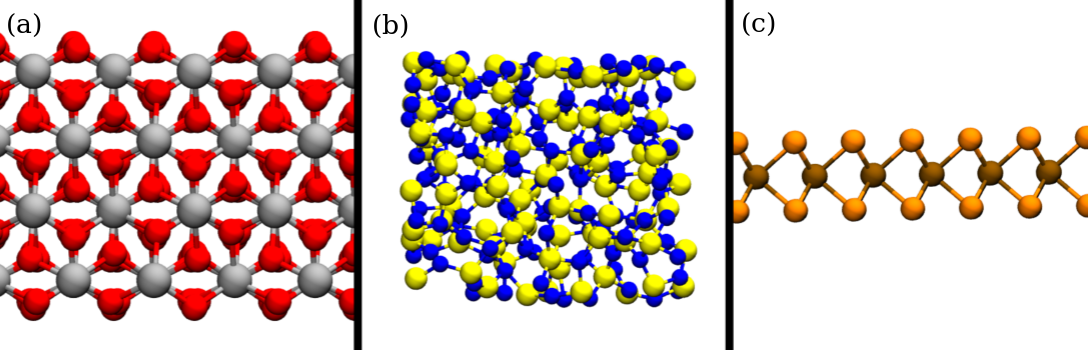
natural occurring aluminum oxide forms a trigonal Bravais lattice called corundum (\(\alpha \)-Al2O3 ), which is shown in Fig. 2.6(a). However,
it can also crystallize in a cubic, a tetragonal and a hexagonal lattice [153].
Figure 2.6: Renderings of different material systems investigated in this thesis. (a) crystalline \(\alpha \)-Al2O3 (b) amorphous Si3N4 (c) two-dimensional WSe\(_2\). Al atoms
are drawn in silver, O in red, Si in yellow, N in blue, W in brown and Se in orange.
Due to the lattice character of the crystal, the distances between atoms in a perfect crystal are precisely determined in equilibrium. A defect, such as a vacancy or an impurity, manifests as an irregularity in the periodic structure
and disrupts the regular lattice arrangement. This disturbance creates localized distortions around the defect, which depend on the surrounding atomic environment. Consequently, different defect types exhibit distinct
characteristics, such as charge transition levels or relaxation energies, allowing a direct comparison with experimentally determined defect properties [154, 116]. This is in strong contrast to amorphous materials as will be outlined in the following.
2.3.2 Amorphous
Amorphous materials are solids which lack long-range order and periodicity and exhibit a disordered atomic structure, as illustrated in Fig. 2.6(b). In electronics, amorphous
materials often form during the fabrication process of layered structures, such as the bulk/oxide heterostructures in metal-oxide-semiconductor field-effect transistor (MOSFET) devices. Typical techniques to create such structures
are physical vapor deposition (PVD) and chemical vapor deposition (CVD). During these processes, the thin film that is grown on the substrate becomes amorphous due to the high deposition rate and the low atomic mobility,
which prevents atoms from diffusing and organizing into a crystalline structure [155, 24].
Amorphous materials can also form when a liquid transitions to a solid by rapid cooling of a melted material. This process is typically simulated with molecular dynamics to obtain realistic amorphous sample structures [156, 53, 4] as further discussed
in Section 3.2.
Experimental identification of defects in amorphous materials is challenging and theoretical studies require extensive statistical analysis to account for the full range of possible defect footprints [4, 53]. Due to the random nature of the atomic structure, defects of the same type can exhibit
varying properties depending on the local atomic environment, meaning that their impact on the electronic device may vary significantly. Additionally, different amorphous sample structures can exhibit varying structural and
electronic properties, such as bond lengths, angles or electronic band gaps. The bond lengths in an amorphous material can not be directly determined with spectroscopy measurements due to the lack of periodicity. Therefore, to
analyze structural properties of an amorphous material, more elaborate techniques such the structure factor are required.
Structure factor
The structure factor \(S\) gives information about the long- and short range order of a material by describing the amplitude and phase of a wave scattered by \(N\) atoms located at position \(\textbf {R}_j\). \(S\) can be
obtained experimentally by x-ray or neutron spectroscopy measurements, or calculated from a sample structure. When an incident beam with wave vector \(\bm {k}_0\) interacts with the investigated sample, the amplitude and
phase of the scattered wave can be described as the sum of the scattered wave vectors from all the atoms.
Here, \(f_j\) is an atomic form factor depending on the spatial density of atom \(j\) and \(\textbf {q} = \textbf {k}_s - \textbf {k}_0\) is the scattering vector according to the wave vector of the scatter beam \(\textbf
{k}_s\). This simple definition assumes elastic scattering and a constant beam throughout the whole sample. Furthermore, this expression neglects refraction, absorption and multiple scattering events. The structure factor is then
defined by the normalized intensity of \(\Psi _s(\textbf {q})\) as given by
To compare the structural properties of amorphous sample structures with experiment, the partial structure factor can be calculated with [157, 158, 159]
Here, \(c_{\alpha (\beta )} = N_{\alpha (\beta )} / N\) is the concentration species \(\alpha (\beta )\), while \(\rho \) is the number density of atoms. The radial distribution function \(g_{\alpha \beta }(r)\)
describes density variations as a function of the distance between particle \(\alpha \) and \(\beta \), where \(R\) is the cutoff radius of \(g_{\alpha \beta }(r)\). Both x-ray and neutron scattering structure factors can be
derived from this expression for amorphous sample structures and validated against experimental scattering data of real amorphous thin films. For this thesis, \(S\) was calculated within the implementation of Quantum
ATK [160] and compared with experimental thin films for \(a\)-Si\(_3\)N\(_4\) and \(a\)-SiO\(_2\) as shown in Fig. 4.2 and Fig. 5.1(a).
Bonding in amorphous materials
Coordination number
A simple method to analyze the bonding in amorphous materials based on geometrical criteria is the coordination number, which refers to the number of bonded neighboring atoms up to an arbitrary defined cutoff radius. The
number of atoms within this radius determines the coordination number, which can vary between different species of atoms. For disordered structures, it is often necessary to give an average coordination number for each atom type,
because not all atoms in the system are necessarily fully coordinated. In \(c\)-Si for example, Si has a coordination number of 4, as every Si atom is bonded to 4 other atoms. In crystalline \(\alpha \)-Si\(_3\)N\(_4\), all Si (N)
atoms have a coordination number of 4 (3), because every Si (N) has four (three) neighboring atoms, while in \(a\)-SiO\(_2\) every Si(O) is four(two)fold coordinated [15]. However, for some amorphous materials such as Si3N4 [54], the coordination
number is not well defined but rather stochastically distributed. Therefore, it varies even within different samples of the same composition as will be discussed in Section 5.
Maximally localized Wannier functions
While the coordination number quantifies the local atomic environment in an amorphous system, it completely neglects the electronic structure, which actually represents the chemical bonding. A bonding analysis based on the
electronic charge distribution can be obtained with maximally-localized Wannier functions (WFs) [161]. WFs are defined by a superposition of Bloch orbitals and
give a complete orthogonal basis set for the electronic wave function. Due to the gauge freedom of Bloch orbitals, the WFs are not uniquely determined and, therefore, different sets can be defined. The maximally localized WFs is
obtained by finding the unitary matrix transition of the occupied Bloch orbitals that minimizes the spread of the WFs in real space [162]. As shown
in [161], the WFs can also be directly obtained from the KS orbitals after a DFT calculation by maximizing the functional
This optimization is done with a steepest decent algorithm where the initial matrices are related to the KS orbitals \(\phi _i\) by \(X_{mn}^{(0)} = \bra {\phi _m} \mathrm {e}^{i 2 \pi x/L} \ket {\phi _n}\), with
\(L\) being the dimension of the supercell.
The positions of the maximally localized WFs indicate the presence of chemical bonds in an atomic system. A WF between two atoms denotes the bonding orbital of a covalent bond created by the hybridization of orbitals from
neighboring atoms. Additionally, the WF is located closer to the more electronegative atom of the bond. For example in amorphous Si, the WF is in the middle between two bonded Si [161], while in silicon nitride the WF is closer to the N than to the Si [53] as demonstrated in
Section 5.2.2. Thus, analyzing the exact positions of the WF is a viable method based on the electronic structure to determine if two atoms in an amorphous system are
actually bonded.
2.3.3 2D materials
Two-dimensional (2D) materials correspond to isolated, planar atomic layers which are thermodynamically stable without dangling bonds [163, 164, 165]. Such single layers can be fabricated by either top-down methods such as exfoliation
extraction from a bulk with the same composition [166] or bottom-up approaches such as polyol synthesis [167]. The extraction method is possible because the atoms within each layer of the host material have strong covalent bonds, while the individual layers in the bulk are only
loosely bound together by comparably weak van der Waals forces.
Naturally, the implementation of 2D layers in electronic devices offers the potential to significantly reduce the device size. Although referred to as 2D materials, some 2D structures are technically not planar but exhibit a finite
lateral expansion. A prominent example of such substances are 2D transition-metal dichalcogenides, which consist of a transition metal layer between two layers of chalcogen atoms, as illustrated for a monolayer of WSe\(_2\) in
Fig. 2.6(c). In contrast, materials such as graphene [163] or hBn [168] crystallize in a single plane and can be considered as truly two-dimensional within a finite thickness of \(\sim 0.5\) nm.
To calculate defect properties in a 2D material with DFT, a single layer is placed in a simulation cell with vacuum space perpendicular to the 2D plane. The applied vacuum layer should be sufficiently thick to avoid interactions
between the periodic images of the 2D material.