|
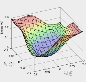
For the post 22nm CMOS technology nodes, strained silicon Ultra-Thin Body (UTB) MOSFETs are considered to be good candidates. As the device feature sizes approach the wave length of free electrons, the influence of quantum mechanical effects gains importance. Besides quantum mechanical tunneling, energy quantization significantly affects the carrier transport in the inversion channel of MOSFETs by the formation of subbands. Hence, the carrier transport occurs on these two-dimensional energy bands. This is particularly true for ultra thin body devices, where the potential well is mainly defined by the geometrical structure. Fundamental transport properties of MOS devices can be derived from cuts through the channel. That way quantum mechanical carrier confinement and electrostatic effects are captured. To solve the Schrödinger equation, the conduction band of unstrained silicon is commonly approximated by three pairs of equivalent valleys located close to the X-points of the Brillouin zone. In modern UTB devices, the dispersion relation is not sufficiently described by the Effective Mass Approximation (EMA). Therefore, an improved self-consistent Schrödinger-Poisson model for the calculation of the electron subband structure of UTB devices has been developed. The proposed approach is based on a two-band k·p Hamiltonian that takes band nonparabolicity, arbitrary strain, and substrate orientation into account. Although it has a small matrix size compared to full-band approaches, an excellent description of the band structure over a wide range of the Brillouin zone is assured. Furthermore, emphasis has been put on the efficiency and accuracy of the numerical, two-dimensional k-space integration of the subbands, which is necessary in order to obtain the carrier concentration. For this purpose, the Clenshaw-Curtis method, which is based on non-equidistant interpolation nodes, is employed. Simulation results of (001) and (110) oriented silicon UTB double gate devices, demonstrate the suitability of the proposed numerical method.
|