|
Bias temperature instability is one of the most important reliability issues in modern MOSFETs. It is observed when a large bias is applied to the gate of an otherwise grounded transistor and results in a drift of crucial device parameters, most notably the threshold voltage. Even after four decades of research, bias temperature instability is still a highly puzzling phenomenon, which has so far eluded our complete understanding. One of the most controversial aspects at the moment is whether interface or oxide charges are the cause of the degradation. Experimental techniques conventionally used to differentiate between these two are difficult to apply, since they rely on modifying the gate bias during measurement, which in turn dramatically accelerates recovery of the degradation. Thus, in order to better understand the phenomenon, the complex degradation/recovery patterns that are observed when the gate bias is modulated need to be understood. This is also mandatory for any estimation of device degradation in a realistic circuit setting. Quite contrary to the latest experimental observations, most modeling approaches published so far have focused on constant gate bias stress and are remarkably oblivious to any recovery of the degradation, which sets in as soon as the stress is removed. In particular, none of these features can be explained by the most-commonly used reaction-diffusion model.
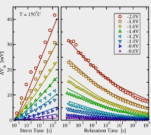
A frequently used assumption is that both oxide and interface states are independently responsible for the total degradation. On the other hand, many researchers have observed a 1:1 correlation between the two. Based on detailed experimental evidence, we have suggested a two-stage model for negative bias temperature instability, which works in quite a similar fashion as interface state generation following irradiation. In state one, charge is trapped in oxygen vacancies close to the silicon interface. Contrary to previous explanations, though, it can be shown that charge is not simply trapped in oxide: in order to accommodate the trapped hole, the lattice relaxes around the trapped charge and forms a defect, most likely an E' center, which can be repeatedly charged and discharged. Only after having been in the neutral state for long enough can the defect fully anneal. Following this charge capture and lattice relaxation, an interface state can be created, for instance by a hydrogen exchange between E' and Pb centers. Experimental evidence for such a connection has been frequently given in literature. So rather than being independent entities, the charges stored in oxide and interface defects become naturally correlated. In particular, after discharging of the recoverable E' centers, the 1:1 correlation between interface and oxide charges can be explained. The model has been validated against experimental data obtained from three vastly different technologies (ultrathick SiO2, thin SiON, and high-k
devices) and very good agreement has been obtained.
|