|
As devices scale towards atomistic sizes, research in silicon electronic device technology investigates alternative structures and materials. As predicted by the International Roadmap for Semiconductors (ITRS), structures will evolve from planar devices into devices that include 3D features, strong channel confinement, strain engineering, and gate all around placement for better electrostatic control on the channel. Alternative channel materials such as Carbon NanoTubes (CNT), NanoWires (NW), and III-V based channel materials are considered as possible candidates for future device technology nodes. For nanoscale dimensions, both atomistic and quantum effects become important in determining the electronic structure and transport properties of the devices.
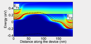
We use the Non-Equilibrium Green's Function (NEGF) formalism for quantum transport simulations and real space atomistic tight-binding techniques (pz, sp3d5s*-SO) to investigate transport properties in CNT, NW and III-V HEMT field-effect transistors. We investigate the effect of physical quantization on the electronic structure of NW field-effect transistors and identified the main electronic structure factors that influence their performance. It was found that structural and quantization below 10nm can severely affect the electronic properties of NW channels by changing the effective masses and altering degeneracies through valley splitting. In addition, different wire orientations can provide different transport properties. We also analyze recent experimental data for III-V HEMT devices using the NEGF formalism and address several issues related to the operation of HEMT devices. Interestingly, to first order, a 60nm HEMT device can be thought as a ballistic channel connected to two series resistances.
The properties of nanoscale devices can be engineered to some degree since the length scale degree of freedom enters the design space. Specifically, the electron and phonon mean free path and scattering length can be altered and new properties can emerge. We use this concept to design new low dimensional thermoelectric devices for more efficient energy conversion.
|