|
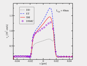
Driven by Moore's law, the device dimensions of modern semiconductors have decreased into the sub-nanometer range. In order to investigate the behavior of such devices and maintain the development cycle, Technology Computer Aided Design tools are very important. For such devices, the commonly used drift-diffusion model becomes more and more inaccurate. A solution is to use more sophisticated models based on Boltzmann's equation, such as the Monte Carlo approach, higher-order moment-based models, or the spherical harmonic expansion approach. The disadvantage of the Monte Carlo (MC) technique is its high computational burden due to the statistical approach, which makes it less suitable for engineering applications. However, the results obtained from the Monte Carlo simulation method are frequently used as a benchmark for other simpler models. For engineering purposes, macroscopic models based on the method of moments such as the drift-diffusion, the hydrodynamic, six moments, or even higher-order models, are adequate approaches for modeling sub-microscopic devices. So far, higher-order transport has been studied using bulk Monte Carlo simulations and has been successfully used in table-based macroscopic transport models for nin-structures. However, since the transport parameters are fundamentally affected by the surface properties and quantization in the inversion layer of, for instance, Ultra-Thin Body (UTB) Semiconductor On Insulator (SOI) MOSFETs, the application of bulk parameters is questionable. In order to describe higher-order transport in inversion layers of a whole device, a 2D non-parabolic macroscopic transport model based on subband MC tables has been developed. The advantage of this method is that inversion layer effects, such as surface-roughness scattering, quantization etc., are inherently considered. To investigate the validity of this approach within short channel devices, crucial transport quantities, such as velocity (see figure), which determines the output current, are compared to results obtained from the device subband MC method. As an example device, a UTB SOI MOSFET with a film thickness of 4nm has been considered.
|