Erasmus Langer
Siegfried Selberherr
Bindu Balakrishna
Oskar Baumgartner
Hajdin Ceric
Johann Cervenka
Otmar Ertl
Wolfgang Gös
Klaus-Tibor Grasser
Philipp Hehenberger
René Heinzl
Hans Kosina
Goran Milovanovic
Neophytos Neophytou
Roberto Orio
Vassil Palankovski
Mahdi Pourfath
Karl Rupp
Franz Schanovsky
Philipp Schwaha
Ivan Starkov
Franz Stimpfl
Viktor Sverdlov
Oliver Triebl
Stanislav Tyaginov
Martin-Thomas Vasicek
Stanislav Vitanov
Paul-Jürgen Wagner
Thomas Windbacher

Vassil Palankovski
Dipl.-Ing. Dr.techn.
palankovski(!at)iue.tuwien.ac.at
Biography:
Vassil Palankovski was born in Sofia, Bulgaria, in 1969. He received the diploma degree in electronics from the Technical University of Sofia in 1993. Afterwards he worked for three years in the telecommunications field. In March 1997, he joined the Institute for Microelectronics at the Technische Universität Wien, where he received the doctoral degree in technical sciences in 2000 and continued as a post-doctoral researcher. In summer 2000, he held a visiting research position at LSI Logic Corporation, Milpitas, California. In 2003, Dr. Palankovski and Dr. Quay published the book Analysis and Simulation of Heterostructure Devices in the Springer Series on Computational Microelectronics. In 2004, he joined Infineon Technologies, Villach, Austria, for half a year as a technology development engineer. Having received the highest Austrian award for young scientists (START-Preis), Dr. Palankovski returned to the Technische Universität Wien in 2005 to establish the Advanced Materials and Device Analysis group. In 2008, he was elected a member of the young curia of the Austrian Academy of Sciences.

Analysis and Simulation of Advanced Heterostructure Devices

A large project (START) on "Simulation of Advanced Semiconductor Devices" funded by the Austrian Federal Ministry for Science and Research (BMWF) through the Austrian Science Fund (FWF) enters into its fifth year.
The project includes several research topics, such as modeling of novel semiconductors (strained Si/SiGe, various III-Vs, as well as the Group IV-VI material systems). The device applications include advanced high-frequency high-power Heterojunction Bipolar Transistors (HBTs) and High Electron Mobility Transistors (HEMTs), as well as quantum wires and high-efficiency solar cells.
Physics-based analytical models for the lattice, thermal, band structure, and transport properties of various semiconductor materials, as well as models for important high-field and high-doping effects taking place in the devices, are derived and implemented in the device simulator Minimos-NT. The models are calibrated against experimental data from our scientific partners. Novel device structures are investigated, designed, and optimized.
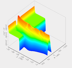
For example, a recent work confirms that multiple avalanching Gunn domains are responsible for the superfast switching observed in GaAs bipolar transistors. Results from two-dimensional hydrodynamic simulations help to understand the generation, transient behavior, and absorption of these domains. The switching includes fairly complex processes: a variation in the number of domains during the transient, a variation in domain amplitude and width, and a variation in the ionization rates within the domains and in the density and energy of the electron-hole plasma between them. The work is very challenging, since the computation of a single transient requires a few weeks, or even months, on the fastest machines currently available, even after major code optimizations.


Electron concentration in the collector of a GaAs bipolar transistor during superfast switching (snapshot at a given time instance).


Home | Activities | Staff | Publications | Sponsors | Music | Contact Us