|
The application of experienced material compositions is evident in the development of modern semiconductors. Miniaturizing the devices pose a challenge to maintain device characteristics. One possible approach is the utilization of mobility enhancement in strained silicon semiconductors. Research has already been undertaken in the characterization and simulation of these stressed semiconductors. To verify these results, the need of a three-dimensional process and device simulation is necessary.
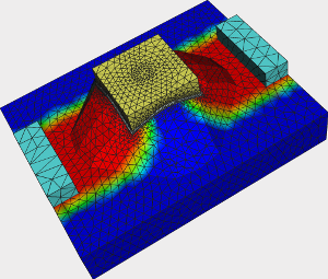
Starting with the given two-dimensional cuts of a test structure in defined directions, a geometric and stress profile was produced. Based on this, a geometric description suitable for a mesh generator was created. Since no mesh description was present at this time, a solid modeling approach was intended. The semiconductor surface of the silicon-dot was described by triangular surface regions. By processing the other materials by geometrical operations, the strained silicon layer placed on the dot, a field-oxide layer, the polysilicon gate and the source, drain and bulk contact were defined. A suitable mesh is crucial for the following device simulation, however, the demands for the mesh are quite oppositional. Generally, the mesh size has to be small to limit the required matrix sizes and, as a result, the simulation times are reduced. On the other hand, the mesh has to be dense enough to achieve accurate simulation results. Particularly under the gate a mesh density in the range of the field oxide thickness is required.
Due to the flexibility of the underlaying tetrahedral mesher netgen, the grid spacing at the oxide-semiconductor interface could be tuned independently, growing towards the outer regions at the bulk, source, and drain contacts.
For the first approach, a constant boron implantation and an analytical phosphorus doping distribution with highly doped islands under the contacts was applied. The stress distributions were interpolated from the given ortho-grid to the unstructured mesh.
Equipped with this adapted layout, the analysis of the device characteristics with Minimos-NT was possible. So far, the impact of stress deviation and different curvature in the border regions, compared to a pure two-dimensional simulation, has been coverable.
|