|
Strain enhancing has become an integral part of improving the performance of modern electronic devices.
Simulation of such devices helps the developer to predict their electric improvement.
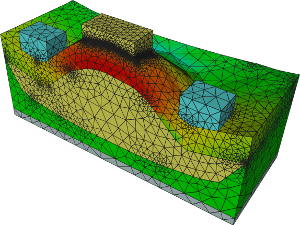
In the illustration, the channel of the device is built in a Si capping layer that is grown on SiGe islands.
The device geometry is supplied by our project partners with the use of a three-dimensional Atomic Force Microscope (AFM) measuring xyz-samples of the semiconductor surfaces.
Unfortunately this data is not useful for device simulation and a technique for extraction of the desired information and building up
the device was developed.
A volume representation of the semiconductor regions has to be achieved. First, the two-dimensional projection of the samples is meshed
by a triangular mesher. Afterwards the third coordinate is reassigned and the triangles are
assembled to valid surface representations of the segments.
Due to the high point density of the input surfaces, a smoothing stage with proper point elimination is performed on these segments.
Afterwards the three-dimensional tetrahedral mesher Netgen is applied.
The mesher interface has no method of structure description by segment boundaries and desired interior
points. Segments must be described by boolean operations of a solid modeler, which is otherwise pretty well suited for the later addition of the
remaining segments. The surfaces can be defined by polyhedral "solids" which have to be combined by boolean operations with the other segments.
The second hurdle, to achieve a high mesh density in the channel region without the possibility of explicit point placement,
was handled by Netgen's built in
point density mechanism. At the oxide surface a small maximal tetrahedron height with growing factor is defined.
In this way the tetrahedrons
under the oxide in the strained silicon layer will start dense and grow towards the peripheral regions, achieving a good resolution in the
channel region.
Afterwards a gate oxide and a polysilicon gate are deposited, source and drain are built as contacts and the substrate contact occurs underneath.
Finally, arsenic and boron doping is implanted and the provided stress profiles are interpolated to the simulation grid.
Provided with this segment description and simulation mesh, the three-dimensional device simulation can begin to compare the characteristics
of the unstrained and strained devices.
|