|
Trap sites in the gate dielectrics of Metal-Oxide-Semiconductor Field Effect Transistors (MOSFETs) play a crucial role in a number
of effects not immediately related to each other. By assuming a
suitable energetic and spatial distribution of trap sites, a model for
excess noise in the drain current of MOSFETs was presented in 1957.
More recently, oxide traps were found to be involved in reliability
issues such as Negative Bias Temperature Instability (NBTI). While with
large-area transistors, the drain current excess noise takes the ubiquitous
1/f spectral shape and NBTI degradation and -recovery proceed as
continuous processes, small-area transistors containing just a handful of
traps show discrete levels in their drain current. In steady-state, these
levels and the abrupt transitions between them are commonly referred to
as Random Telegraph Noise (RTN). With NBTI degradation and
recovery, although the device is then in a pronounced non-equilibrium,
similar transitions between discrete levels can be observed.
By carrying out a number of carefully designed stress/relaxation
experiments, it is possible to extract the statistical parameters of the
individual traps of the transistor, provided that the latter is small enough
such that the drain current steps can be assigned unambiguously to the traps.
This is aided by the non-uniform drain current distribution in the channel of
a real MOSFET, causing individual traps to cause distinctive drain current
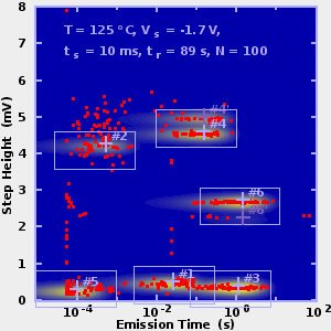
steps. Binning of the emission times and step amplitudes into a
two-dimensional histogram called a spectral map reveals marked clusters of
events. Since the underlying physical process is poissonian, the temporal
probability distribution of events is exponential, while the step height is
distributed as a narrow gaussian. Unfortunately, trapping a carrier at one
site perturbes the current distribution in the channel, modulating the
characteristic step amplitudes of other traps. This effect can be observed
in a number of measurements, and has to be taken into account when
extracting the statistical parameters of the traps.
Varying the stress time shows that the clusters do not move within the
spectral map, i.e. step amplitude and emission time are independent of stress
time, ruling out, for example, diffusive processes. On the other hand, the amplitude
of the probability distribution of a particular trap increases with stress
time, consistent with the picture that for a trap to show an emission event
it has to capture a carrier within the preceding stress phase, which becomes
more probable when this stress phase is longer. From a row of experiments
with different stress times and the resulting probability amplitudes, it is
therefore possible to extract the capture time constants of the traps.
Repeating this block of experiments at different temperatures and/or
different stress voltages and/or different relaxation voltages, the
dependencies of the emission- and capture times on these parameters can be
investigated.
|