|
High Electron Mobility Transistors GaN-based (HEMTs) are considered for
high-power, high-frequency applications in a wide temperature range.
Reliable software tools for DC and AC simulations are required for the
further development and optimization of the devices. Since the
drift-diffusion transport model is not able to deliver accurate results for sub-micron
devices, we employ the hydrodynamic approach. Appropriate material models, which
account for the peculiarities of the material systems, are developed and calibrated
against experimental data and results from our own Monte Carlo simulations. We
focus on GaN, AlN, InN, and their respective alloys.
We analyze different structures such as single and double heterojunction
AlGaN/GaN HEMTs, as well as novel InAlN/GaN transistors. The latter provide
higher polarization charges without the drawback of high strain, thus
performance superior to AlGaN/GaN structures is predicted.
Our work also includes the optimization for various applications
(high-power, high-frequency or high-breakdown), involving different enhancement
techniques. We account for all relevant physical effects. Our sets of
material and model parameters are validated against experimental data in a wide
temperature range. Studies of the device performance at elevated
temperatures are performed.
Due to the intense interest in normally-off devices, several approaches are
currently being analyzed. One such approach is the addition of an InGaN cap
layer, which raises the conduction band of the AlGaN/GaN interface. Another
approach is the recessed-gate technique, which also improves the RF
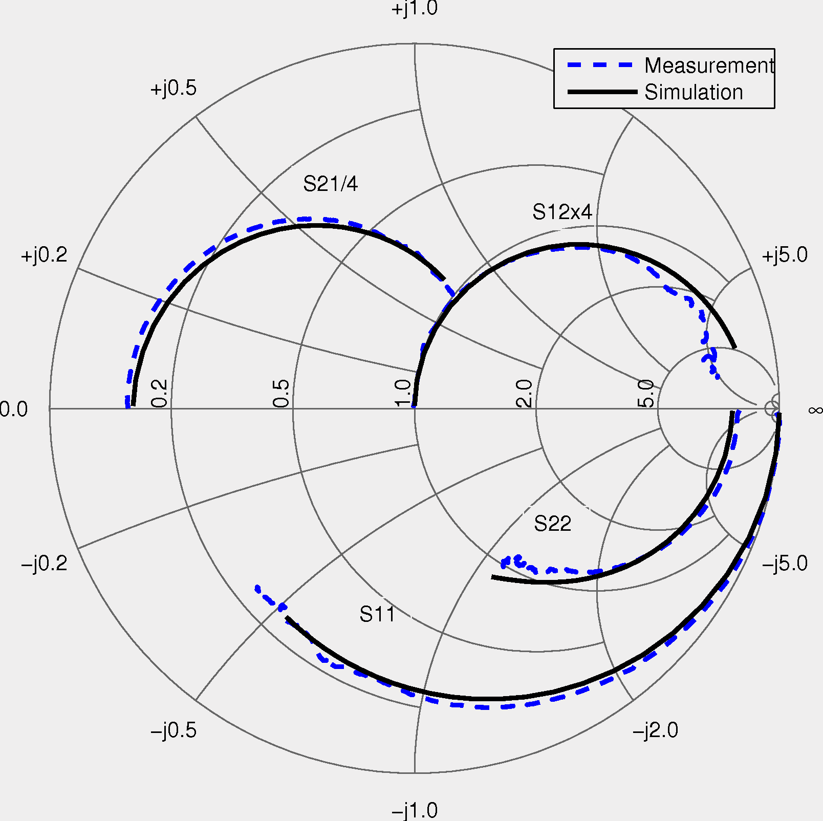
performance. We have achieved excellent predictive results for the
S-parameters for devices of different technologies and geometries. The impact of the
material properties and device geometry on the small signal equivalent
circuit elements is studied.
High power DC-DC inverters are used in the hybrid electric vehicles that
have entered the market over the last couple of years. For such automotive
applications, high breakdown voltage as well as low on-resistance and the
capability to operate at high temperatures are key requirements. Our
calibrated simulator is thoroughly suitable for the design and optimization of such
devices.
|