|
Hot Carrier (HC) degradation has been the subject of intensive research for over three decades and still remains one of the most important concerns in the field of transistor reliability. Initially, transistor dimensions were scaled faster than the power supply, resulting in increasing electric fields in the channel and, as a consequence, severe HC degradation. For modern MOSFETs employed for logic applications, operating voltages already lie below those related to the threshold energy for interface state generation and thus the halt of degradation for scaled devices was expected. However, in practice even extremely-scaled devices are subject to HC degradation.
Present knowledge reveals that HC degradation is due to interface state generation by rupturing the Si-H bonds at the silicon/silicon dioxide interface. The rupture is triggered by energy transfer of carriers in the channel to the Si-H bond. One may roughly separate "hot" and "colder" carriers assuming that in the first case bond-breakage is dominated by a Single-Particle (SP) process while in the second case a Multiple-Particle (MP) mechanism is responsible for the damage. This concept suggests that for long-channel devices the SP-mechanism dominates degradation, while in scaled devices the MP-component may become more pronounced. Therefore, while modeling HC degradation, one should consider competing SP- and MP-processes and, hence, collect information about the carrier energy Distribution Function (DF).
At the same time, the charge captured by the created interface states determines the degradation, which may be significantly different from the net concentration of traps (Nit). In fact, just charged traps distort the transistor band diagram and play the role of Coulombic scattering centers. The occupational statistics of traps is firmly linked to the trap Density-Of-States (DOS) and to the position of the quasi-Fermi level of carriers populating these states. In order to explain the double-power law behavior observed during degradation, two types of traps associated with the SP- and MP- processes have been suggested. This concept is also supported by calculations obtained from density functional theory. We thus distinguish between SP and MP-related traps by using different densities of states for these mechanisms.
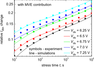
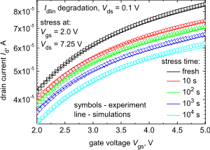
Consequently, a complete model for HC degradation should capture two key issues, i.e. the generation of the interface states by two competing mechanisms and their occupation at real device operation conditions. The first issue is related to the distribution of carriers over energy and thus reflects the interrelation between "hot" and "colder" charge carriers. In order to properly consider this matter, we employ a full-band Monte-Carlo device simulator that allows us to calculate the carrier energy distribution function for the particular device architecture. As for the second issue, we calibrate the model in a manner to reproduce degradation of the whole transfer characteristics (Ids-Vgs) for different stress and operational conditions. This strategy allows us to collect information about the trap density of states. We show that traps related to the multiple-carrier mechanism are located at higher energies with respect to those created by the single-carrier mechanism. The model calibrated according to this scenario allows us to describe degradation of the transistor transfer characteristics with very good agreement.
|