|
As devices scale down towards atomistic sizes, research in silicon electronic and thermoelectric device technology investigates alternative structures and materials with enhanced properties. For transistor device applications, as predicted by the International Roadmap for Semiconductors (ITRS), structures will evolve from planar devices into devices that include 3D features, strong channel confinement, strain engineering, and gate all around placement for better electrostatic control on the channel. A possible alternative channel material for future electronic devices is the silicon NanoWire (NW). For other applications, such as thermoelectric devices, silicon NWs have attracted a lot of attention after the realization that length scale provides an additional degree of freedom in engineering the electronic and thermoelectric transport properties of devices. Thermoelectric devices (especially devices based on silicon channels) traditionally operate on low efficiency. Nanostructured thermoelectric devices with enhanced performance compared to their bulk counterparts, however, have recently been realized. Silicon NWs with performance two orders of magnitude higher than bulk silicon have been demonstrated, and initialized hopes for high performance silicon thermoelectrics.
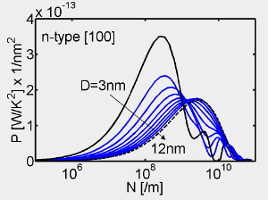
We use the atomistic tight-binding sp3d5s·-SO model to investigate the transport properties of silicon NWs. We investigate the effect of physical quantization on the electronic structure of NW channels and identified the main electronic structure factors that influence their performance. It is found that structural quantization below 10nm can severely affect the electronic properties of NW channels by changing the effective masses, changing the curvature of the bands, and altering degeneracies through valley splitting. Different wire orientations have different transport properties. This length and orientation degree of freedom in engineering silicon NW channels, offers optimization possibilities for nanostructured electronic and thermoelectric devices. It is found that the [110] oriented NWs provide high performance for both n-type and p-type applications. The [100] channels exhibit poor p-type performance, while the [111] channels poor n-type performance. In the case of thermoelectric devices, it is found that as the diameter decreases below 6nm, the power factor increases (see figure). It is also found that channels with a large number of valleys nearby in energy are beneficial for the power factor and enhance thermoelectric performance. Therefore, subband engineering through appropriate surface quantization of NWs can be beneficial for low dimensional thermoelectric devices for more efficient energy conversion.
|