|
Systems with two dimensional quantum confinement such as nanowires / nanowire-Field Effect Transistors (FETs), FinFETs and gate-all-around structures are believed to be one of the most promising candidates for next generation devices that will replace the current planar MOSFETs and allow further device scaling. However, the quantum nature of the charge carriers in these novel devices needs to be considered carefully.
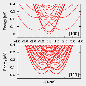
An accurate description of the subband structure is essential to understand the way nanowire devices operate. The Hensel-Hasegawa-Nakayama model, a two band k·p model of the conduction band, can deliver such an accurate description as far as electrons are concerned.The bulk band description is adapted to take confinement into account by replacing two out of three components of the k-vector with derivatives. Treating the remaining k-vector component as a parameter, a two dimensional partial differential equation is obtained and solved numerically within the domain of the nanowire cross section, assuming the wave functions to vanish outside the silicon core (Dirichlet boundary conditions). The numerical solution of the resulting eigenvalue problem is solved efficiently using the ARPACK library, which provides a significant performance improvement over other solver routines when only a few of the total number of eigenvalues and eigenvectors are needed. The computational code was implemented within the Vienna Schrödinger Poisson (VSP) 2.0 simulation framework.
An intriguing feature of the two band k·p model is that effects of strain on the band structure can be easily taken into account by adding two additional terms to the Hamiltonian. Using the stiffness tensor for silicon, the application of stress along various axes was investigated. Also, different crystallographic orientations for nanowire growth as well as circular and rectangular cross section shapes were assumed for the calculations; the results were found to agree reasonably well with subband structures obtained from tight binding calculations.
|