The simulation of source and drain domain build-up in modern MOSFETs is an explictly three-dimensional TCAD problem due to several effects. First there are silicon/silicon-dioxide, silicon/polysilicon and polysilicon/silicon dioxide interfaces whith a specific structure in each spatial dimension. Segregation effect take place at these interfaces and influence formation of the junction through the pile-up phenomena. Furthermore, the silicon/silicon-nitride and silicon/silicon-dioxide interfaces are places of point defect generation and annihilation. These interface processes have stronger impact on the point defect dynamics than bulk processes and thus influence considerably the diffusion behavior of the dopants. Here again the three-dimensional structure of the interfaces between silicon and others materials of the MOSFET structure is the cause of three-dimensional dopant profiles broadening.
In the following sections we present three-dimensional simulation results. The simulations are carried out with the FEDOS tool based on the diffusion models and PDE discretization and linearization schemes presented in previous sections.
Here we use the vacancy-only model (Section 3.3.3) in combination with the segregation model (Section 3.5.3) to simulate the behavior of phosphorus dopants in the vicinity of the silicon/silicon-dioxide interface.
The extrinsic phosphorus diffusivity is modeled according to [6] assuming that phosphorus atoms diffuse with neutral and negatively charged vacancies,
![$\displaystyle D_{P}=\Bigl[3.85 e^{-3.66 \text{eV}/kT} + 4.44 \Bigl(\frac{n...
....2\Bigl(\frac{n}{n_i} \Bigr)^2 e^{-4.37 \text{eV}/kT}\Bigr] \text{cm}^2/s.$](img674.png) |
(3.146) |
The extrinsic concentration of the electrons ![]() is calculated using (3.13).
is calculated using (3.13).
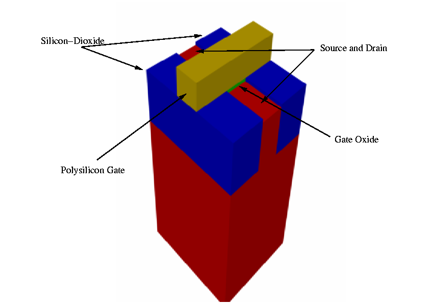
The considered MOSFET structure is displayed on Figure 3.3. An initial phosphorus profile is calculated by means of implatation with a dosis
![]() cm
cm![]() and energy
and energy ![]() keV (Figure 3.4).
The ion-implantation simulation is carried out with the simulator MCIMPL-II [39,40].
keV (Figure 3.4).
The ion-implantation simulation is carried out with the simulator MCIMPL-II [39,40].
|
a)
b)
|
|
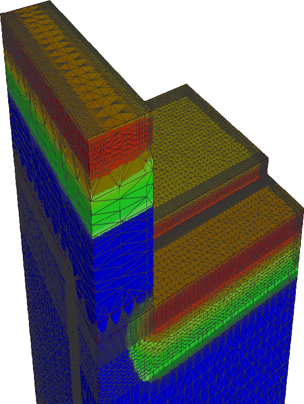
The mesh used for the simulation is presented in Figure 3.5. Since we have expected higher gradients of dopant concentration in the vicinity of silicon/silicon-dioxide interface the simulation mesh is refined in this area with increased number of points in the direction ortoghonal on the silicon/silicon-dioxide interface.
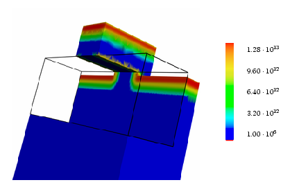
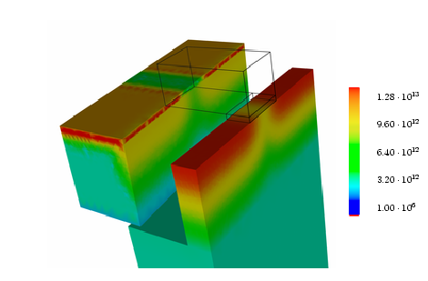
After a diffusion time of ![]() min the dopants have spread deeper into the silicon bulk and penetrated into silicon-dioxide, as can be seen from the Figure 3.7.
min the dopants have spread deeper into the silicon bulk and penetrated into silicon-dioxide, as can be seen from the Figure 3.7.
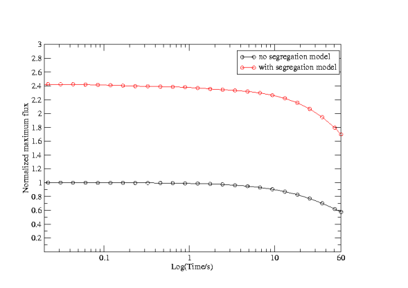
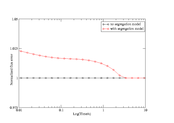
The characteristic pileup in the vicinity of the silicon/silicon-dioxide interface can be observed on the basis of the behavior of maximal phosphorus concentration flux and flux error, calculated on the basis of discussion presented in Section 2.9. A pileup effect, as part of the segregation of dopants on the silicon/silicon-dioxide interfaces, is regularly observed in experiments [41,42,43].
For comparison the simulation is carried out with and without the segregation model. The diffusion conditions at the silicon/silicon-dioxide interface produce from the very beginning distinctively higher concentration gradients. The curves presented in Figure 3.6a are normalized to the maximum concentration gradient in the case where no segregation model is applied. The presence of the silicon/silicon-dioxide interface causes a more than 2.4 times larger phosphorus concentration gradient. However, due to a carefully chosen mesh (Figure 3.5) no significant increase of the flux error is observed.
The real significance of three-dimensional diffusion simulation in present process technology lays in the influence of the boundary conditions. The physics at the silicon/silicon-dioxide and silicon/nitride interface has a strong impact on the dynamics of point defects and thus on the diffusion of dopants [33,28,20].
It has been established [34,21,20] that the interactions at these interfaces can be described by a simple phenomenological model, given by (3.67) and (3.68), which still allows the appropriate description of two basic effects: silicon boundary as perfect reflector for point defect and silicon boundary as perfect point defect sink. Some researchers argue the complete dominance of surface processes over bulk processes [34].
In order to illustrate three-dimensional effects and capabilities of the numerical schemes presented in Sections 3.8.3 and 3.8.5 we use a setup of process steps preeceding the diffusion process step as follows. For performing the three-dimensional process simulation flow the topography simulator TOPO3D [44,45] has been used. Deposition and etching process steps have been carried out with the empirical model of TOPO3D.
The following pictures show as example a sequence from the three-dimensional simulation of typical CMOS technology process flow.
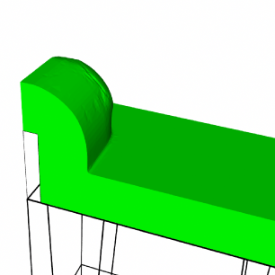
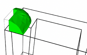
Before source/drain formation, a deposition of the conformal Si![]() N
N![]() layer is carried out (Figure 3.8).
The thickness of this layer will determine the thickness of the sidewall spacer and it is used to optimize device characteristics [5].
Subsequentially, the deposited Si
layer is carried out (Figure 3.8).
The thickness of this layer will determine the thickness of the sidewall spacer and it is used to optimize device characteristics [5].
Subsequentially, the deposited Si![]() N
N![]() layer is anisotropically etched (Figure 3.9), leaving a sidewall spacer along the edge of the polysilicon.
layer is anisotropically etched (Figure 3.9), leaving a sidewall spacer along the edge of the polysilicon.
In the prepared structure an initial arsenic profile is introduced with the multi-dimensional ion implantation simulator MCIMPL-II [39,40].
Implanted is the dosis of
![]() cm
cm![]() with the energy of
with the energy of ![]() keV.
keV.
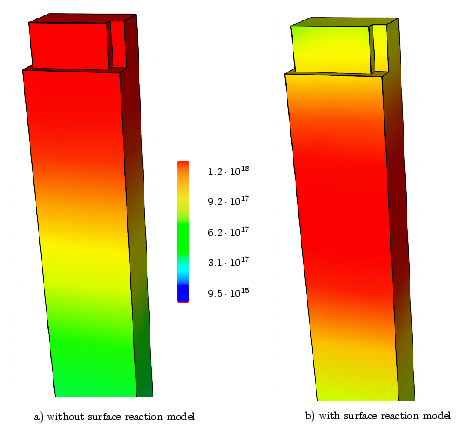
For comparison reason the simulation is performed simultaneously using the Mulvaney-Richardson model (Section 3.4.2) with the surface recombination model (Section 3.5.4) and without it. To obtain high nonequilibrium dynamics of the point defects the one-plus model is applied.
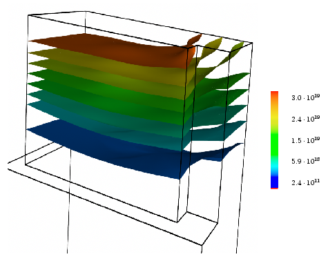
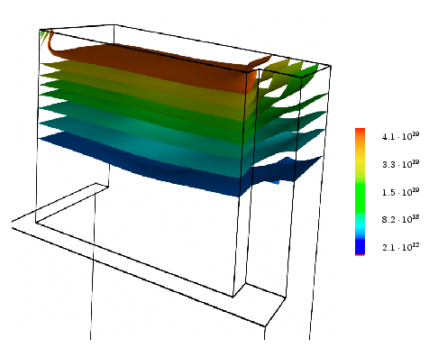
The simulation result for the interstitial concentration without surface reaction model is presented in Figure 3.10a and with the surface reaction model in Figure 3.10b. In both cases the simulations have been carried out at 950 ![]() C for the duration of approximately 1 s.
Figure 3.10b shows a significant lowering of the interstitial profile not only directly in the vicinity of the silicon/silicon-dioxide interface but also deeper in the bulk. The silicon surface acts as sink of the interstitials, trying to reduce the concentration level from that given by the one-plus effect to the equilibrium level.
Since the silicon/silicon-dioxide interface has an explicitely three-dimensional shape, the resulting interstitial profile will also show three-dimensional spreading.
C for the duration of approximately 1 s.
Figure 3.10b shows a significant lowering of the interstitial profile not only directly in the vicinity of the silicon/silicon-dioxide interface but also deeper in the bulk. The silicon surface acts as sink of the interstitials, trying to reduce the concentration level from that given by the one-plus effect to the equilibrium level.
Since the silicon/silicon-dioxide interface has an explicitely three-dimensional shape, the resulting interstitial profile will also show three-dimensional spreading.
Since the interstitals are the main vehicles of enhanced arsenic diffusion, the dwindling of interstitals reduces the depth of the diffused arsenic profile. This can be clearly seen from the Figure 3.11 (no surface recombination) and Figure 3.12 (with surface recombination). The good example of the experimental results confirming the strong influence of the silicon/silicon-dioxide interface on the transient enhanced diffusion can be found in [46].
|
|