« PreviousUpNext »Contents
Previous: 4.2 Evolution of fixed oxide charges Top: 4 Charge accumulation in high temperature processing steps Next: 4.4 Interpretation of the results
4.3 Analysis of minority carrier traps using photo-assisted CV
In a wide band gap semiconductor like SiC, the impact of minority carriers is not visible in the CV curve due to the extremely small intrinsic carrier density. Therefore, the interface charge density  was extracted using photo-assisted capacitance
voltage measurements as described in Section 1.3.5.
was extracted using photo-assisted capacitance
voltage measurements as described in Section 1.3.5.
Fig. 4.6 shows a photo-assisted CV measurement after processing step  . Starting in accumulation at 15 V, the
gate voltage is swept to deep-depletion in the dark (cyan). While the bias is held in deep-depletion, the sample is illuminated with 350 nm light to populate the inversion layer, which results in an increase of the capacitance.
Minority carriers are generated and move to the interface, where they are trapped in available interface states. Afterwards, the light is turned off and the gate voltage is swept back to accumulation in the dark, which results in the red
curve. As can be seen, a voltage shift occurs in the CV curve due to the trapped minority carriers. The dashed lines represent the simulated CV-curves of the MOS system [131]. For the simulation of the illuminated curve (red),
. Starting in accumulation at 15 V, the
gate voltage is swept to deep-depletion in the dark (cyan). While the bias is held in deep-depletion, the sample is illuminated with 350 nm light to populate the inversion layer, which results in an increase of the capacitance.
Minority carriers are generated and move to the interface, where they are trapped in available interface states. Afterwards, the light is turned off and the gate voltage is swept back to accumulation in the dark, which results in the red
curve. As can be seen, a voltage shift occurs in the CV curve due to the trapped minority carriers. The dashed lines represent the simulated CV-curves of the MOS system [131]. For the simulation of the illuminated curve (red),
 remains at the value of the dark-curve and the
interface trap density is increased until the simulated and the measured CV curves match. The photo-assisted CV measurements for all high temperature processing steps are shown in Fig. 4.7. For
remains at the value of the dark-curve and the
interface trap density is increased until the simulated and the measured CV curves match. The photo-assisted CV measurements for all high temperature processing steps are shown in Fig. 4.7. For  , the photo-assisted data is missing because such a
measurement was not possible in combination with the mercury probe. The number of oxide traps and the density of interface states extracted from all measurements is given in Fig.
4.8.
, the photo-assisted data is missing because such a
measurement was not possible in combination with the mercury probe. The number of oxide traps and the density of interface states extracted from all measurements is given in Fig.
4.8.
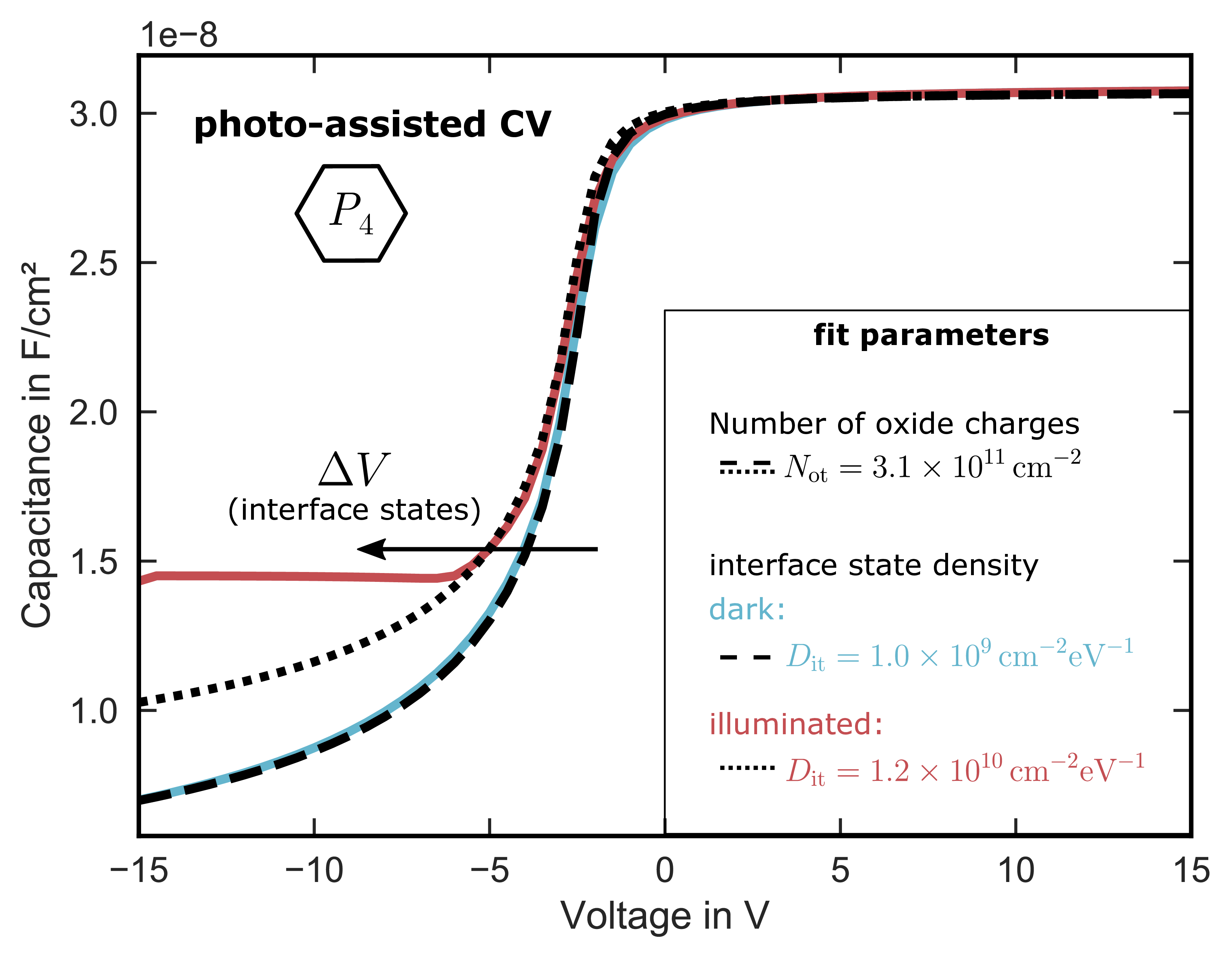
Figure 4.6: Photo-assisted CV-measurement after high- processing step . The curve after the sample was illuminated is shown
in red. The number of oxide traps remains identical at 3.1 × 10¹¹/cm2 for both fits (black). Due to the generation of minority carriers in the photo-assisted measurement, the impact of the on the capacitance is visible. The dotted black
line shows a simulation of the illuminated curve using an interface state density of 1.2 × 10¹⁰/(cm2 eV).
processing step . The curve after the sample was illuminated is shown
in red. The number of oxide traps remains identical at 3.1 × 10¹¹/cm2 for both fits (black). Due to the generation of minority carriers in the photo-assisted measurement, the impact of the on the capacitance is visible. The dotted black
line shows a simulation of the illuminated curve using an interface state density of 1.2 × 10¹⁰/(cm2 eV).
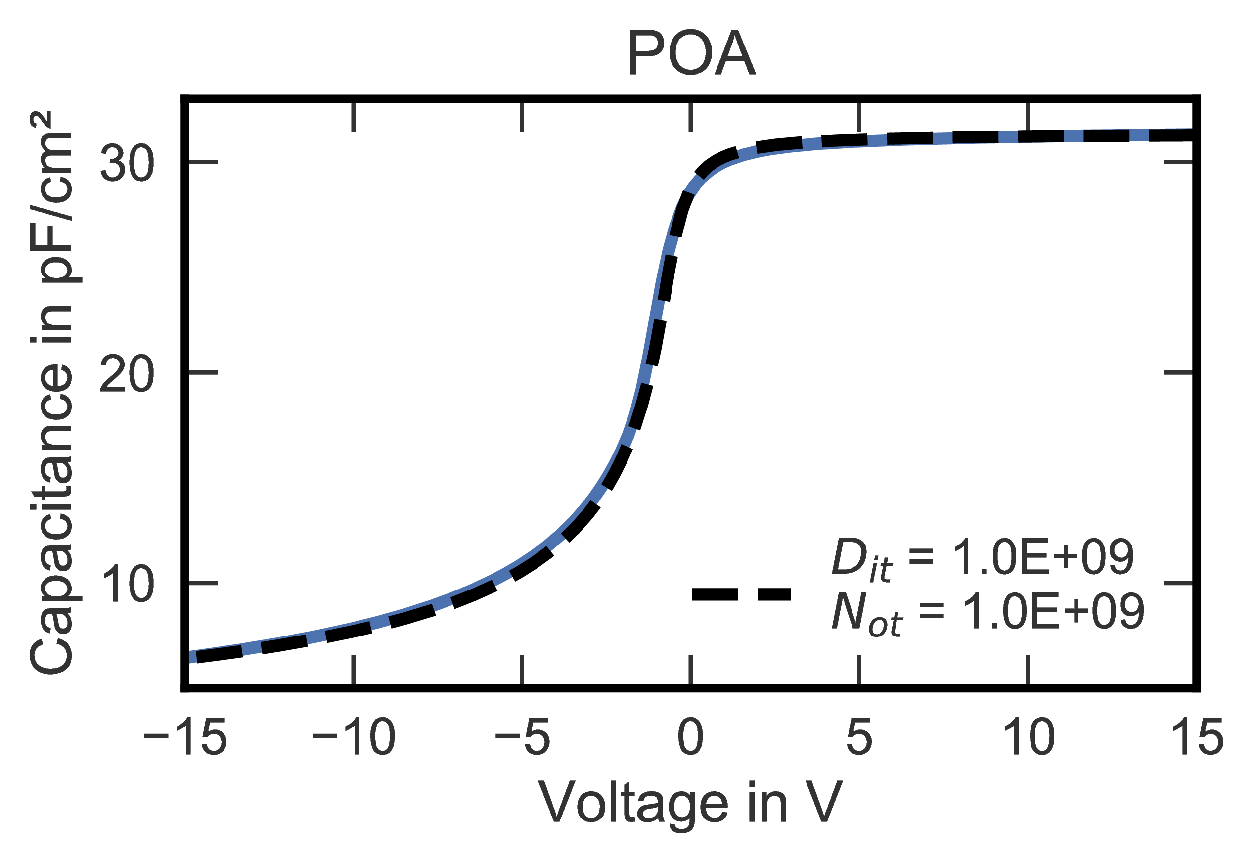
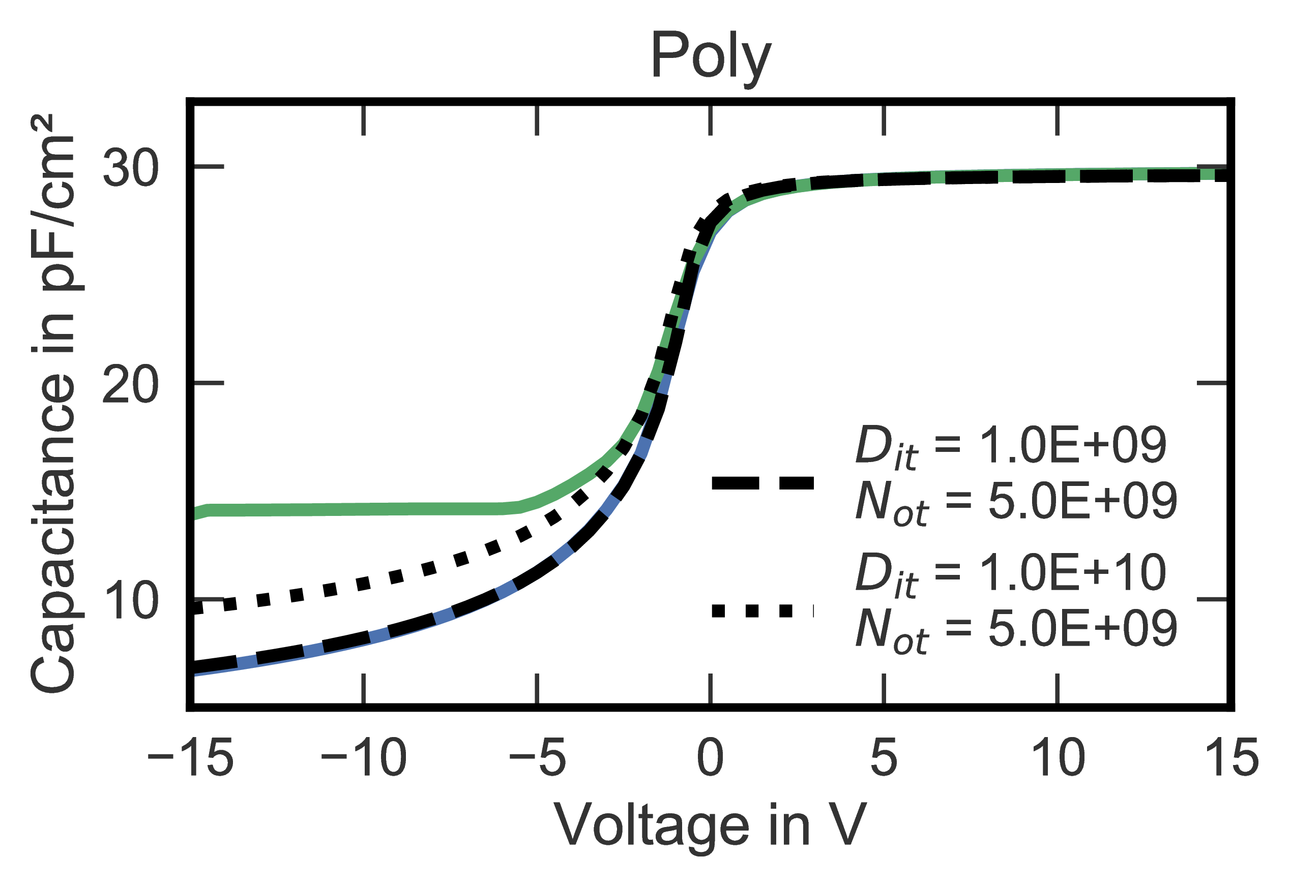
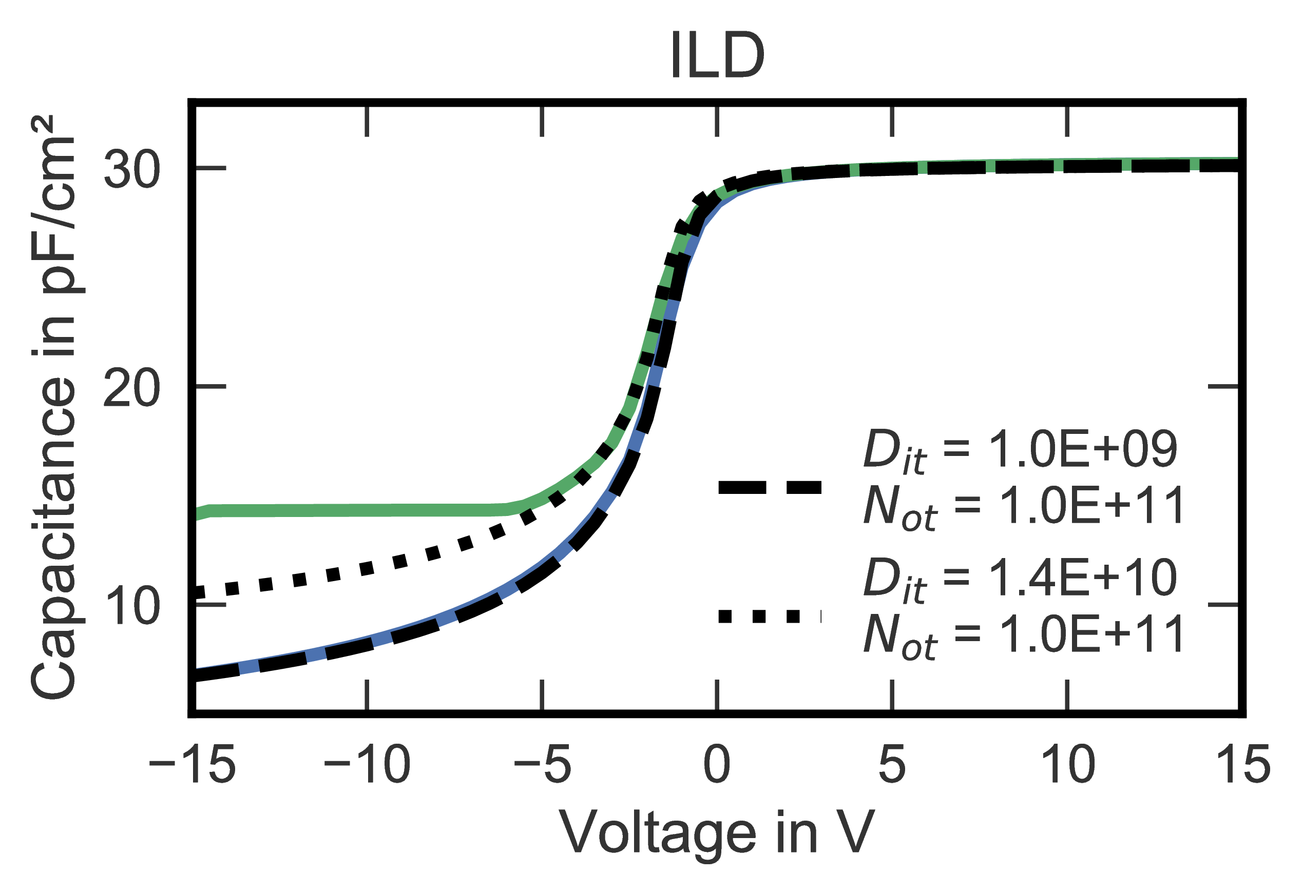
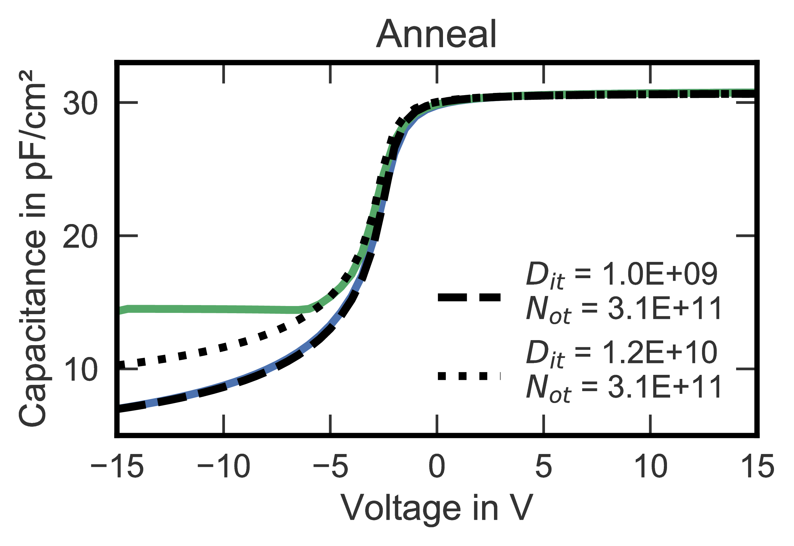
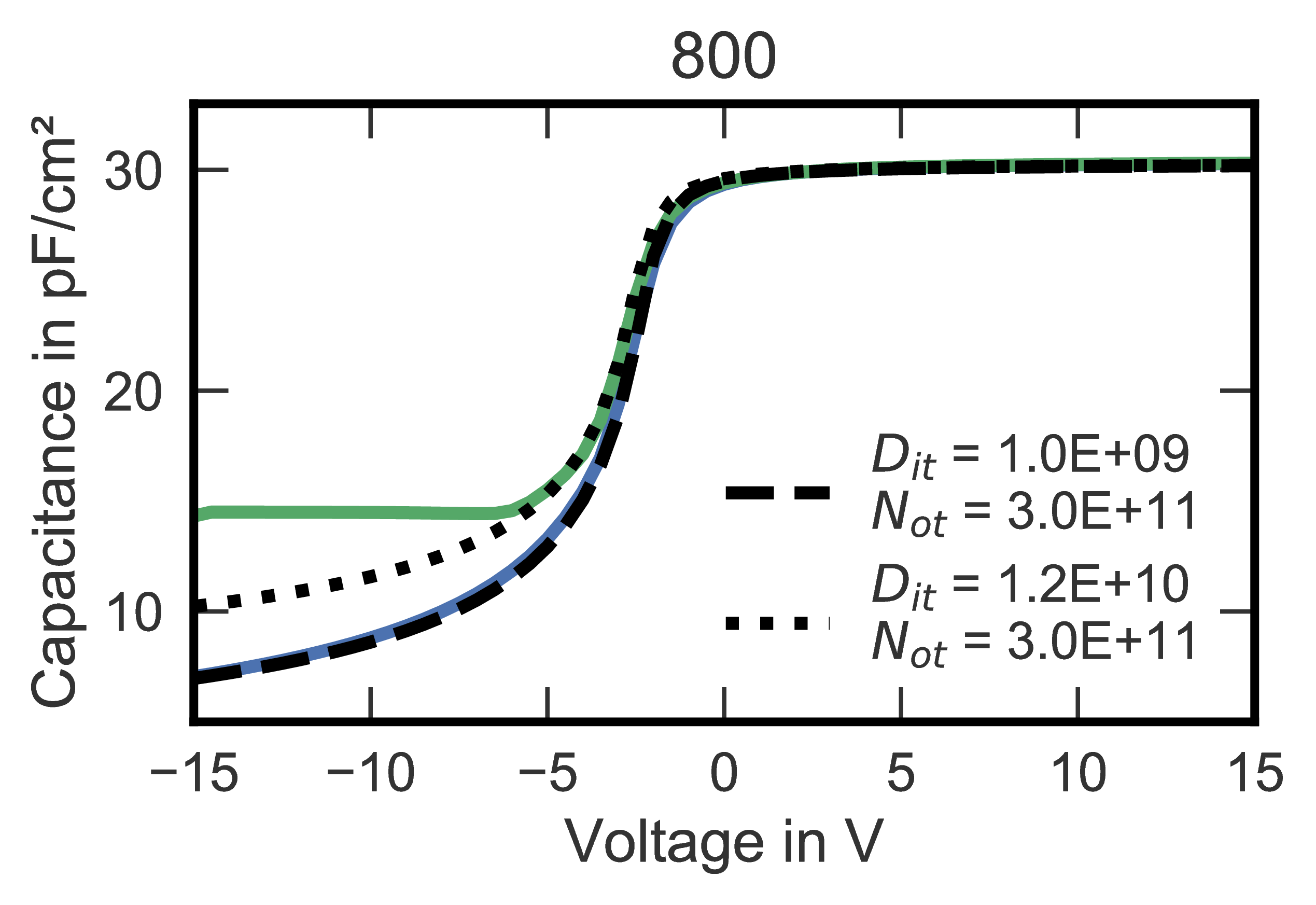
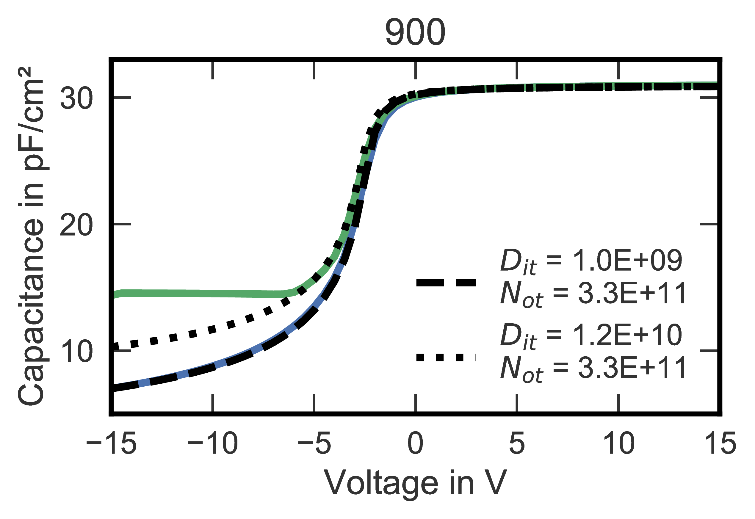
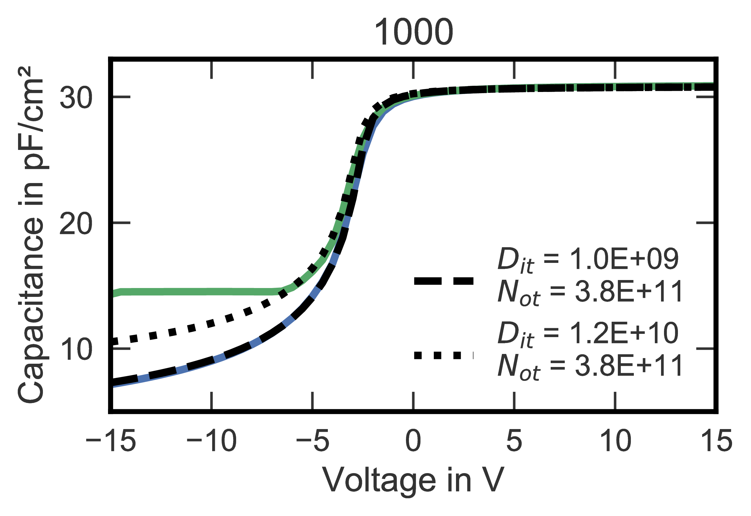
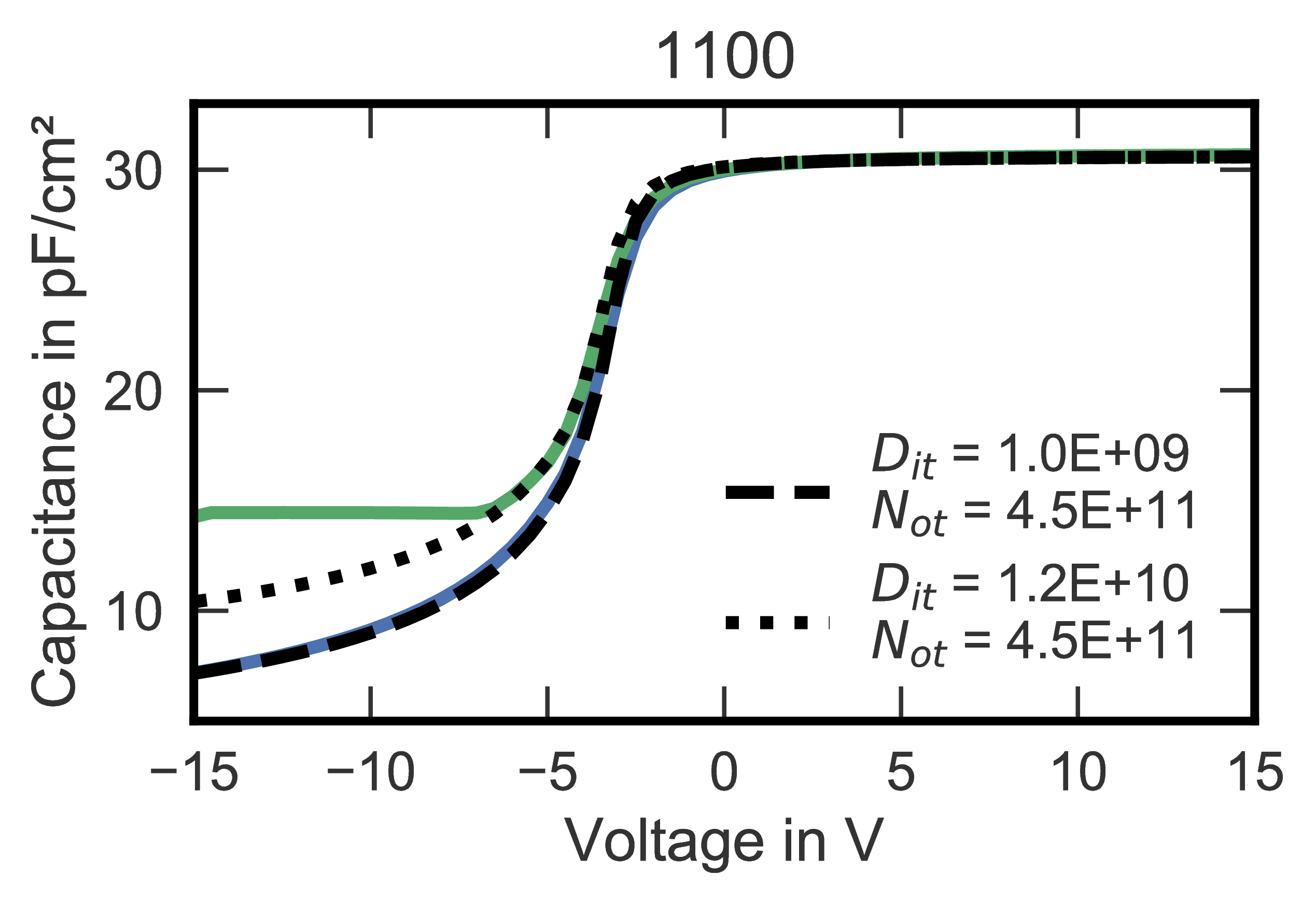


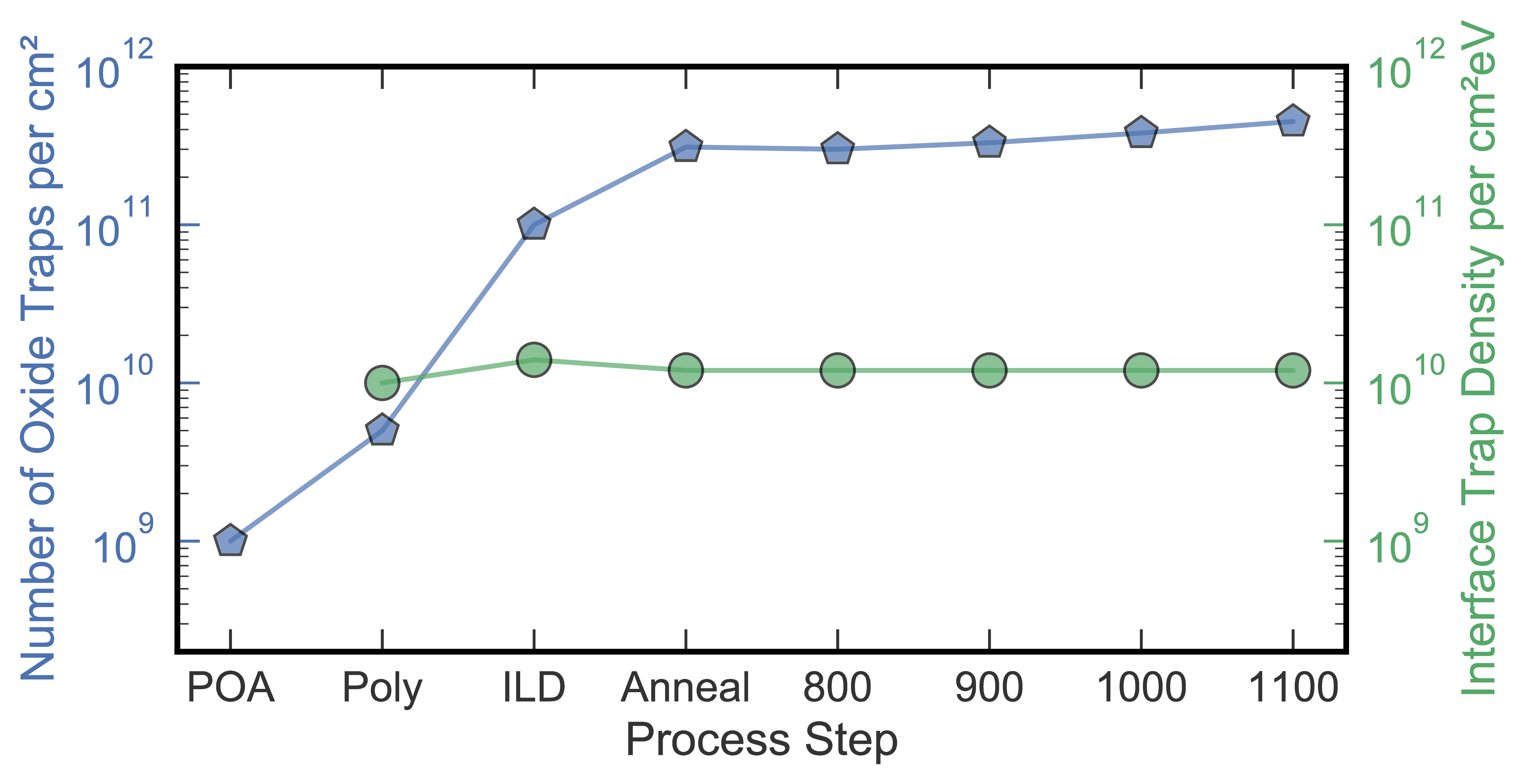
Figure 4.8: Impact of high-temperature processing steps on the total number of positive oxide charges (left-axis, blue) and the interface trap density
(right-axis, green). Unlike the , which increases from  to
to  ,
the interface trap density does not change with increasing thermal budget and remains constant at approximately
,
the interface trap density does not change with increasing thermal budget and remains constant at approximately  throughout processing.
Previous: 4.2 Evolution of fixed oxide charges Top: 4 Charge accumulation in high temperature processing steps Next: 4.4 Interpretation of the results