« PreviousUpNext »Contents
Previous: 1.2 Detrimental Effects in MOS Devices Top: 1 Introduction Next: 2 On the first Component: the Subthreshold Hysteresis
1.3 Methodology
To understand the impact of various trapping centers on the electrical performance and reliability of SiC devices, numerous parameters were extracted using sophisticated measurement techniques. A brief overview on the available experimental setup and on how these electrical parameters were extracted is given in this section.
1.3.1 Measurement system
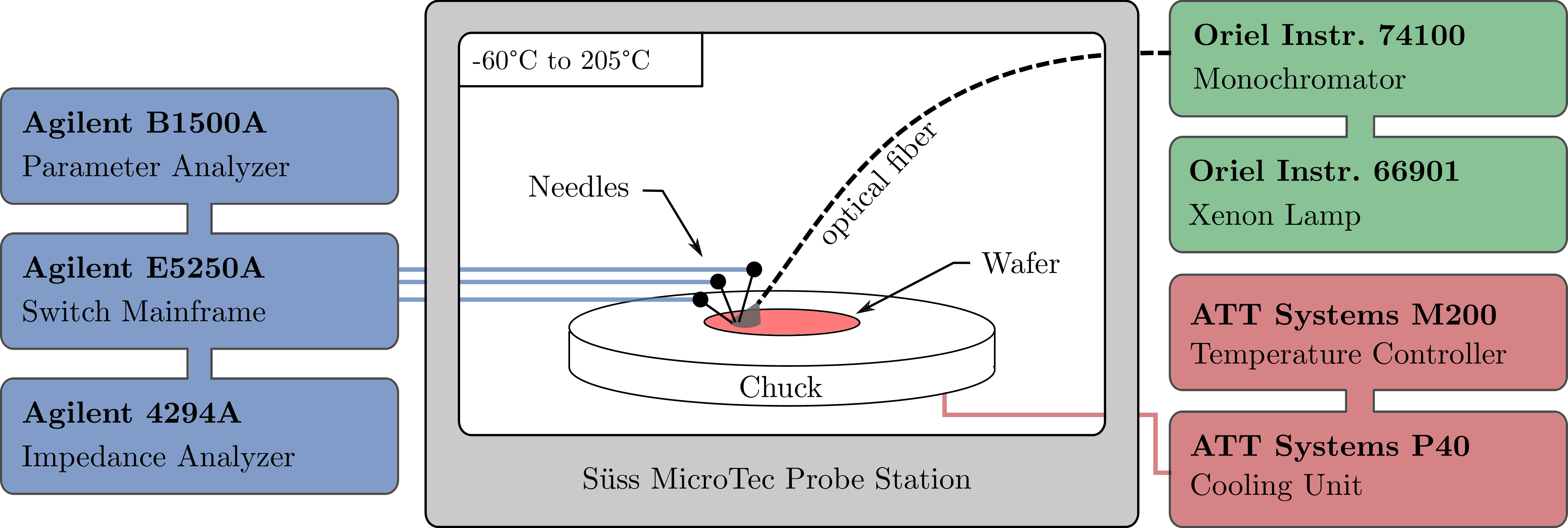
An overview on the available measurement equipment for all investigations in this thesis is given in Fig. 1.11. All measurements were performed using an Agilent B1500A parameter analyzer, which includes 4 high-resolution source-measurement units (SMUs) and one high-power SMU. All SMUs are connected to an Agilent E5250A switching matrix. For capacitance-voltage measurements an Agilent 4294A impedance analyzer was used, which is also connected to the switching matrix. An Oriel Instruments 66901 300 W xenon lamp in combination with an Oriel Instruments 74100 monochromator was used for measurements which require light at a specific wavelength (see Section 1.3.5). All measurements were performed within an Süss MicroTec probe station, where the temperature is controlled via an ATT Systems M200 temperature controller and an ATT Systems P40 cooling unit.
1.3.2 Layout considerations of SiC-power MOSFETs
Unlike in silicon power-MOSFETs, where the contribution of channel resistance  to the total on-resistance
  is negligible, the contribution of to the total in SiC-MOSFETs is significant. Here up to
approximately 50 % of the total on-resistance originates from the channel resistance due to the higher interface trap density and very low drift layer resistance. This results in the need for an increased die size, which
consequently raises the chip costs due to the very expensive base material (
is negligible, the contribution of to the total in SiC-MOSFETs is significant. Here up to
approximately 50 % of the total on-resistance originates from the channel resistance due to the higher interface trap density and very low drift layer resistance. This results in the need for an increased die size, which
consequently raises the chip costs due to the very expensive base material ( for a 150 mm wafer).
Therefore, decreasing using different crystal-planes with higher
mobility and shrinking the pitch size is of high importance for SiC based power-MOSFETs.
for a 150 mm wafer).
Therefore, decreasing using different crystal-planes with higher
mobility and shrinking the pitch size is of high importance for SiC based power-MOSFETs.
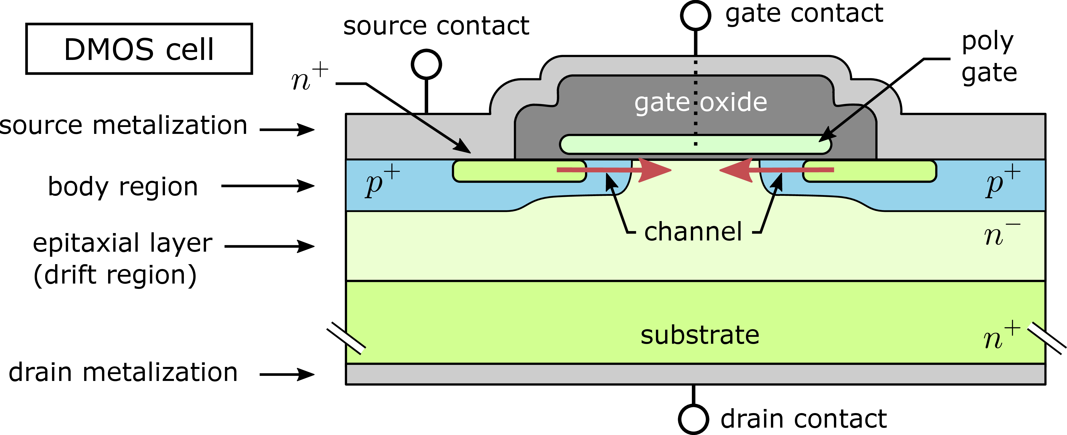
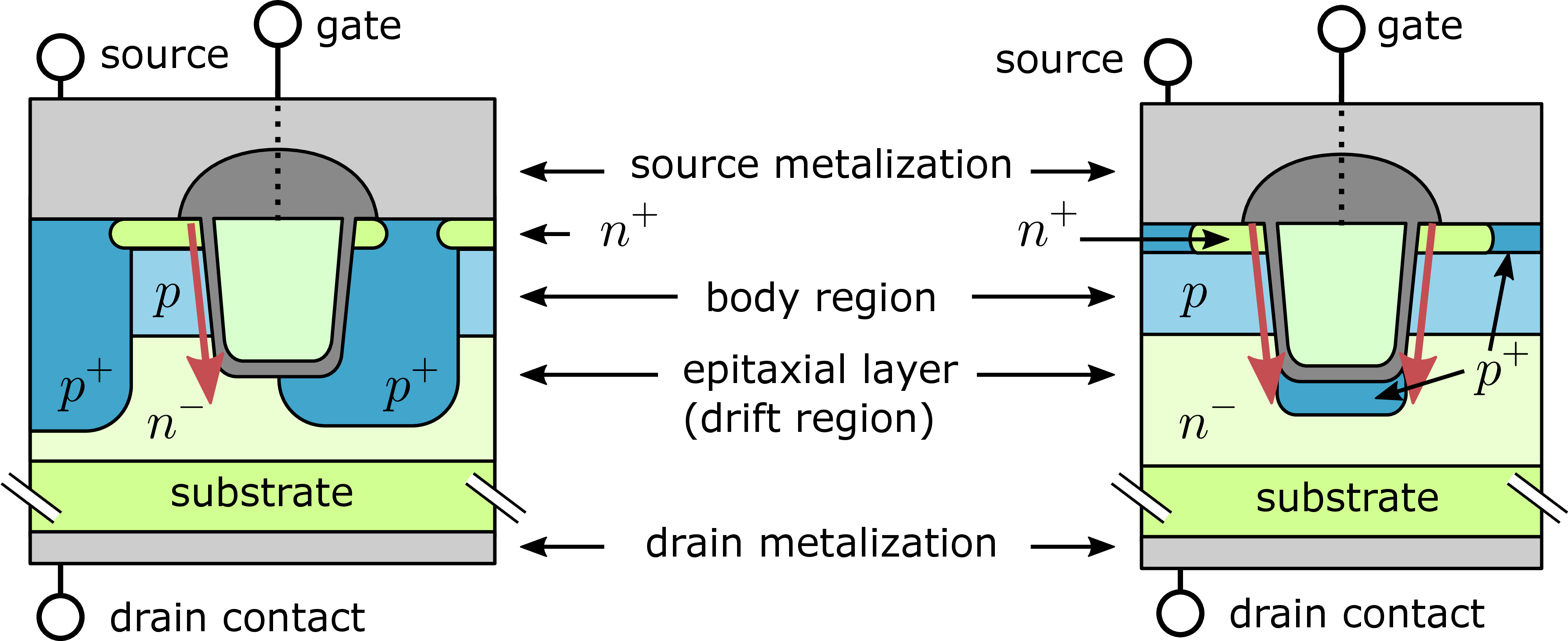

Typical device layouts used in commercially available SiC power MOSFETs are given in Fig. 1.12 and Fig. 1.13. A typical
DMOS design is shown in Fig. 1.12 with the inversion channel (red-arrows) forming on the (0001)-crystal plane (or Si-face). The trench designs (sketched in Fig. 1.13) enable a smaller pitch size, and furthermore take advantage of the higher mobility on the non-polar crystal planes along the  -axis of the 4H-SiC crystal [74]. However, these trench devices require a
  doped region to shield the insulator at the bottom
of the trench from the high electric fields, which arise in the
doped region to shield the insulator at the bottom
of the trench from the high electric fields, which arise in the  doped epitaxial drift layer in the off-state of the device due to the high drain
potential usually applied in power applications [71–73, 75].
doped epitaxial drift layer in the off-state of the device due to the high drain
potential usually applied in power applications [71–73, 75].
As will be shown in Chapter 2, the number of fast interface states with a fully reversible charge state depends strongly on the crystal plane of the inversion layer, and therefore on the device layout.
1.3.3 Transfer Characteristics
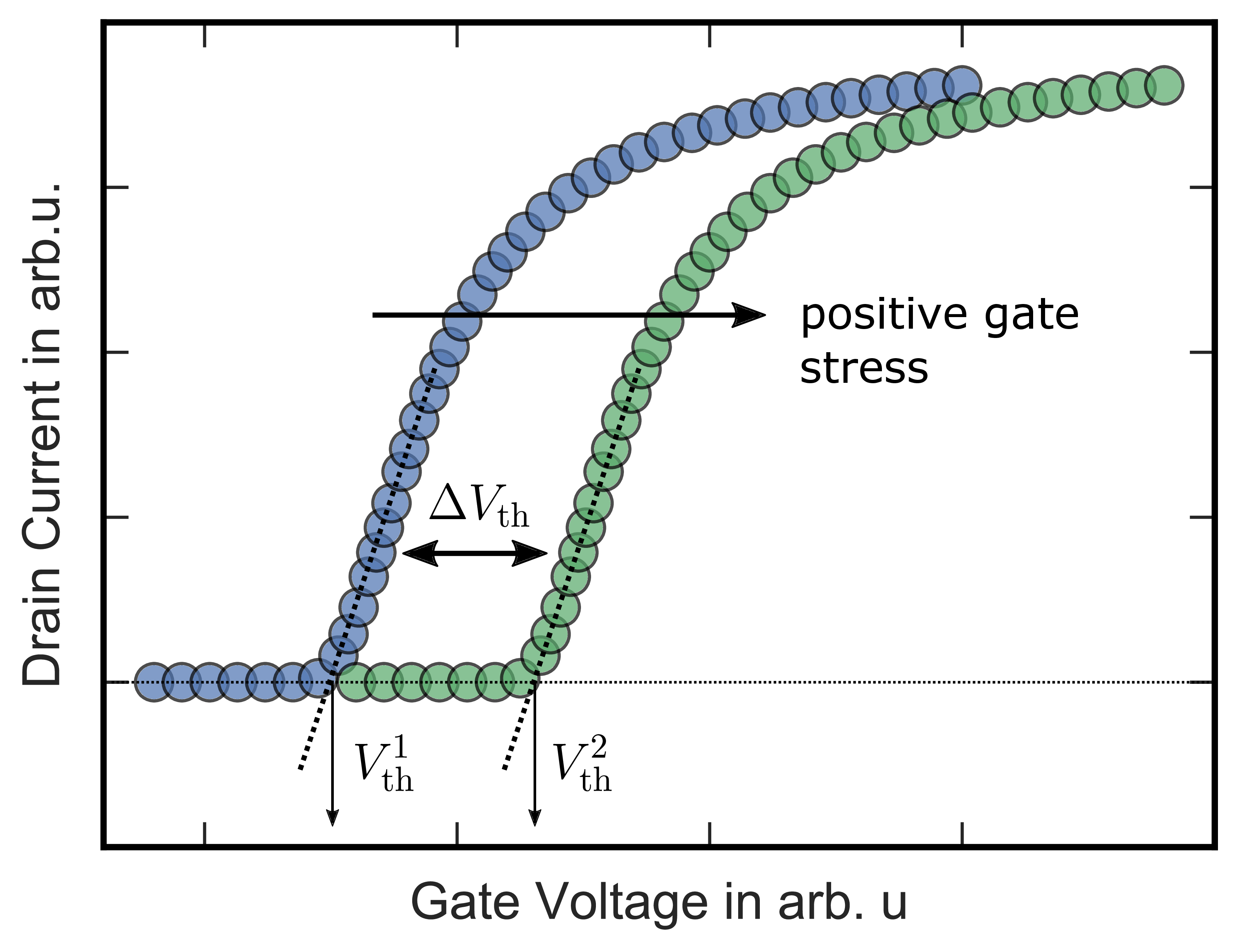
The transfer characteristics (ID -VG s) represent the dependence of the drain current  on the gate voltage
  at a fixed drain voltage
  . Fig. 1.14 shows typical transfer characteristics of a SiC nMOSFET before (blue) and after a high temperature gate stress for several thousand seconds (shifted, green). The threshold
voltage
. Fig. 1.14 shows typical transfer characteristics of a SiC nMOSFET before (blue) and after a high temperature gate stress for several thousand seconds (shifted, green). The threshold
voltage  , as a key parameter of a MOSFET, can be
extracted from the ID -VG s in manifold ways [76–81]. In this work, is extracted using either a linear extrapolation
(as indicated in Fig. 1.14), or is extracted via a defined readout current (e.g.
1 mA) at fixed drain voltage.
, as a key parameter of a MOSFET, can be
extracted from the ID -VG s in manifold ways [76–81]. In this work, is extracted using either a linear extrapolation
(as indicated in Fig. 1.14), or is extracted via a defined readout current (e.g.
1 mA) at fixed drain voltage.
As already discussed in Section 1.2.1, a positive/negative bias stress results in a positive/negative threshold voltage shift  , respectively. Assuming a parallel shift of the
transfer characteristics after bias stress, which is usually the case for SiC-nMOSFETs, is given by
, respectively. Assuming a parallel shift of the
transfer characteristics after bias stress, which is usually the case for SiC-nMOSFETs, is given by

and the total number of charges trapped during the stress  can be easily obtained from the shift of the
threshold voltage via
can be easily obtained from the shift of the
threshold voltage via

with the oxide capacitance  .
.
The transfer characteristics are furthermore used for the evaluation of the low-field mobility  using the method of Ghibaudo [78]. He derived
the linear function
using the method of Ghibaudo [78]. He derived
the linear function

with the transconductance  and Ghibaudo’s definition of the threshold
voltage
and Ghibaudo’s definition of the threshold
voltage  . From (1.9), is extracted as a fitting parameter from the
slope of the linear function
. From (1.9), is extracted as a fitting parameter from the
slope of the linear function  as indicated in Fig.
1.15 and Fig. 1.16. Note that in this thesis the term mobility always refers to the low-field mobility unless otherwise stated.
as indicated in Fig.
1.15 and Fig. 1.16. Note that in this thesis the term mobility always refers to the low-field mobility unless otherwise stated.
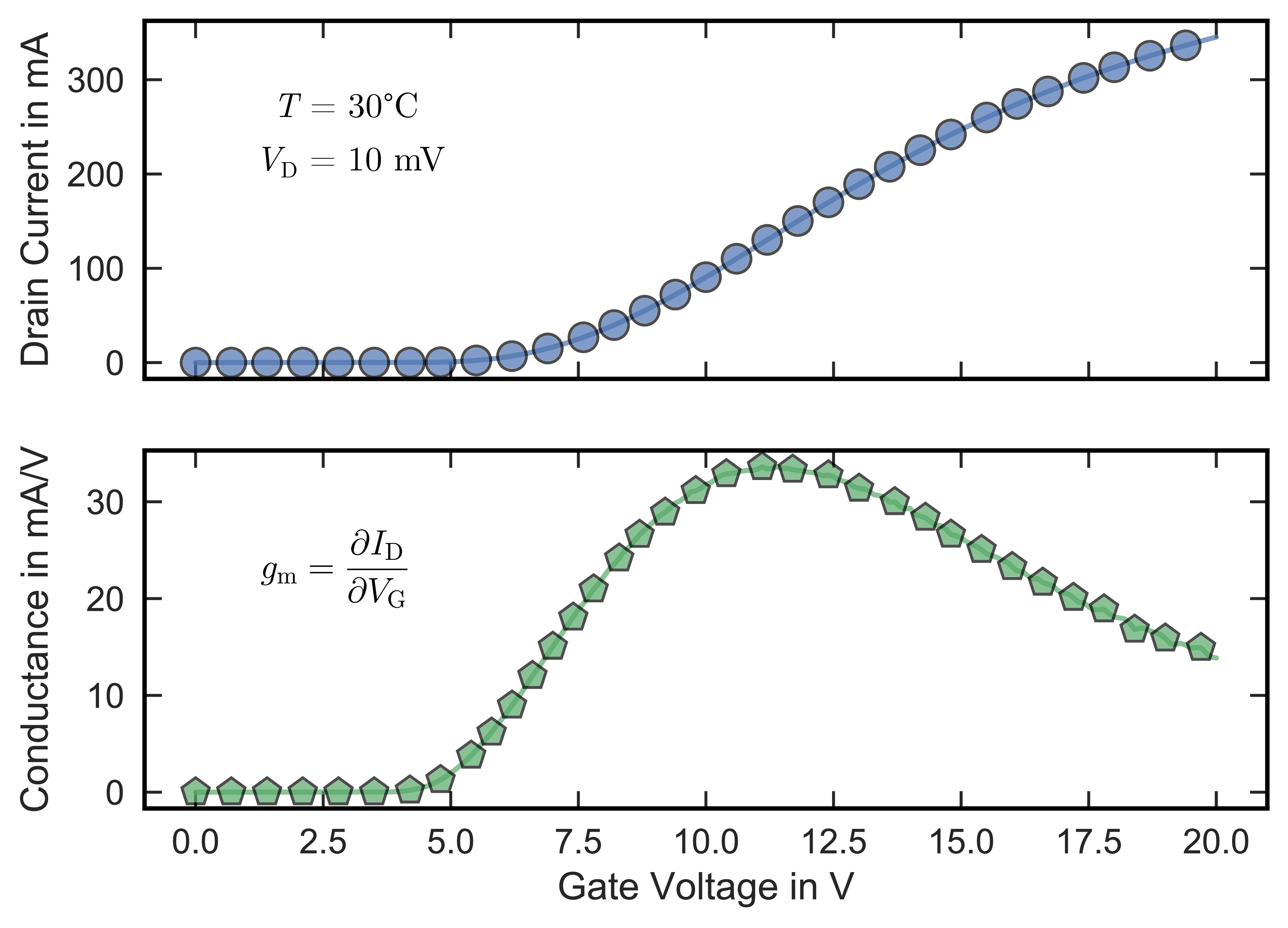
Figure 1.15: Typical drain current (blue, top) and transconductance (green, bottom) characteristics of a MOSFET.
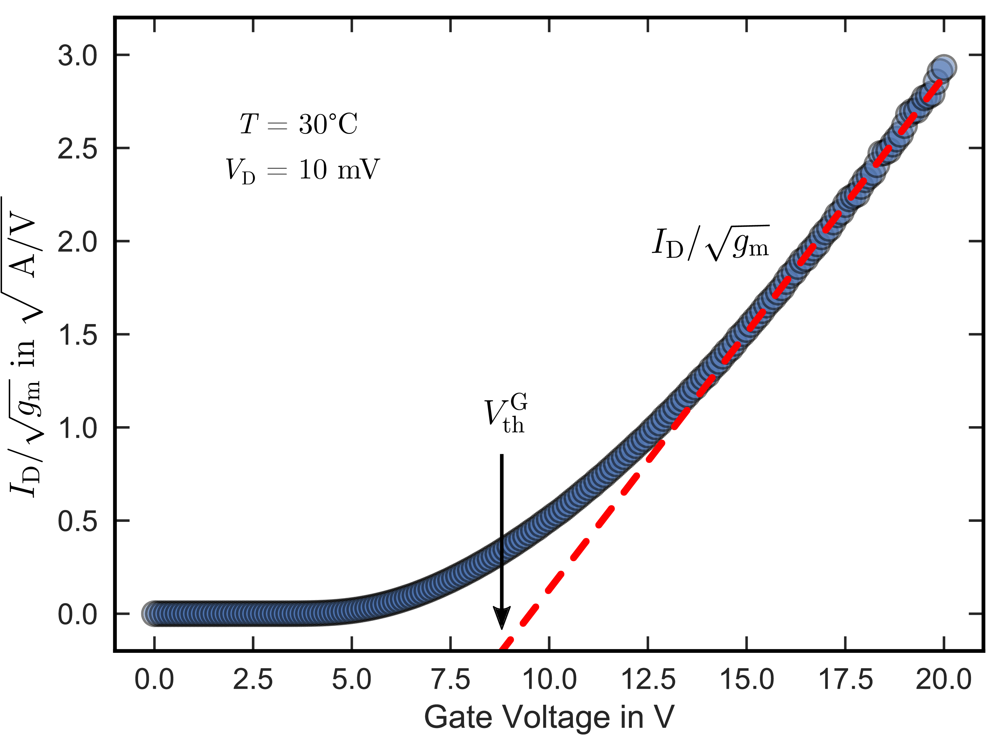
Figure 1.16: Typical / characteristic illustrating the param-
eter extraction via a fit of (1.9) (dashed, red) according to the method of Ghibaudo [78].
characteristic illustrating the param-
eter extraction via a fit of (1.9) (dashed, red) according to the method of Ghibaudo [78].
1.3.4 Charge Pumping
Charge pumping (CP) is an electrical measurement method which was proposed by Brugler and Jespers in 1969 [82]. The technique is very well suited for the quantitative determination of interface and border states in MOSFETs and was recently demonstrated on SiC based devices [29, 83–86]. The next paragraph will give a short introduction to the measurement technique. More detailed information is given in [82, 87, 88].
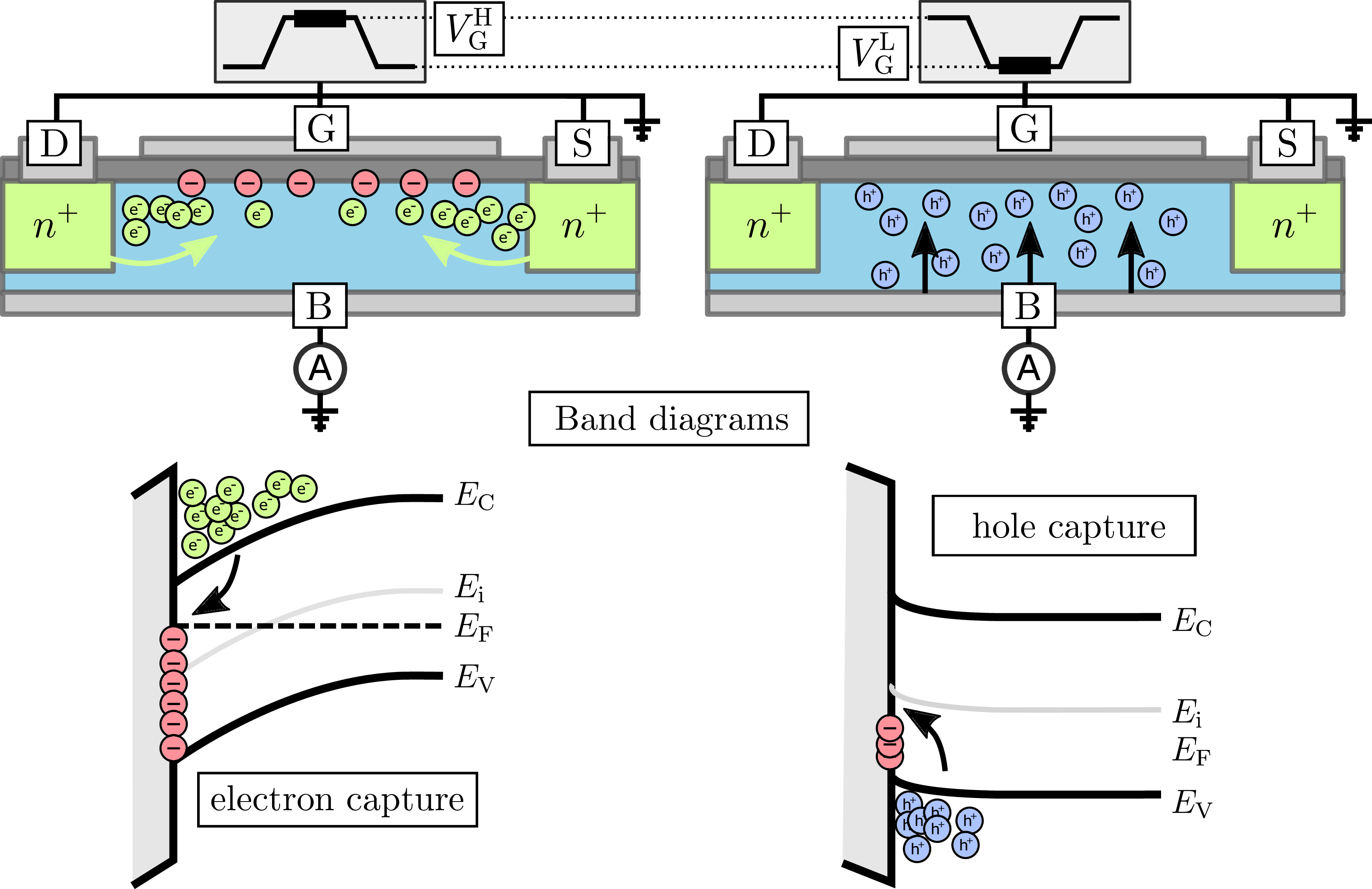
Figure 1.17: Basic scheme of a CP measurement on a n-channel MOSFET. Left: during the high-level of the gate pulse, an inversion channel forms and minority carriers (electrons) are captured in interface/border states (red). Right: during the low-phase of the gate pulse, these trapped electrons recombine with incoming holes from the substrate resulting in an net current flow (= charge pumping current) from the bulk to the source/drain terminals.
The basic connection scheme of a CP measurement is sketched in Fig. 1.17 for an n-channel MOSFET. While source, drain and bulk terminals are grounded, the gate is pulsed at a
frequency of several kHz from accumulation to inversion. During the high-phase of the gate pulse at  , electrons from source and drain are injected
into the channel region of the device. Most of these electrons remain delocalized (free) in the semiconductors conduction band (green), while some get captured in interface or border states (red). As soon as the gate is switched back
to accumulation at
, electrons from source and drain are injected
into the channel region of the device. Most of these electrons remain delocalized (free) in the semiconductors conduction band (green), while some get captured in interface or border states (red). As soon as the gate is switched back
to accumulation at  , delocalized electrons flow back to the source or
drain regions, while most of the trapped electrons remain captured during the falling edge of the gate pulse. These remaining trapped electrons recombine with incoming holes (blue) during the low-phase of the gate pulse, which
results in a net current flow from source/drain to the bulk. In typical charge pumping measurements the gate is pulsed with frequencies ranging from 10 kHz to 1 MHz. Therefore, electrons are repeatedly "pumped"
from the conduction band to the valence band via interface/border states resulting in an effective charge pumping current
, delocalized electrons flow back to the source or
drain regions, while most of the trapped electrons remain captured during the falling edge of the gate pulse. These remaining trapped electrons recombine with incoming holes (blue) during the low-phase of the gate pulse, which
results in a net current flow from source/drain to the bulk. In typical charge pumping measurements the gate is pulsed with frequencies ranging from 10 kHz to 1 MHz. Therefore, electrons are repeatedly "pumped"
from the conduction band to the valence band via interface/border states resulting in an effective charge pumping current  at the bulk terminal. The maximum charge
pumping current
at the bulk terminal. The maximum charge
pumping current  is directly proportional to the total number of
trapped charges per unit area
is directly proportional to the total number of
trapped charges per unit area  at the semiconductor-insulator interface
according to
at the semiconductor-insulator interface
according to

Here,  represents the effective gate area,
  is the frequency of the gate pulse and
  is the elementary charge.
Spectroscopic Charge Pumping
Spectroscopic charge pumping is a tool for the measurement of the energetic distribution of interface traps in MOS systems, which was proposed by Van den Bosch and Groeseneken in 1991 [89]. It is based on the fact that the
mean density of interface states  is always given within a well
defined energetic fraction of the band gap according to
is always given within a well
defined energetic fraction of the band gap according to

This energetic range within the band gap is called the active energy window  given by

with the band gap  , the thermal drift velocity of electrons and
holes,
, the thermal drift velocity of electrons and
holes,  and
and  , the capture cross section of electrons and holes,
 and
and  , the charge-pumping threshold and flatband
voltages
, the charge-pumping threshold and flatband
voltages  and
and  , the amplitude of the gate pulse
  and the rise and fall times of the gate pulse,
 and
and  .
.
The upper boundary of is given by

whereas the lower boundary of is given by

It is important to note that in (1.13) and (1.14), also the drift
velocities  , the capture cross sections
  , and the effective density of states in
the conduction band
, and the effective density of states in
the conduction band  and valence band
  depend on
  . Therefore, the upper and lower boundaries of can be easily adjusted by changing the
temperature or the rise and fall times of the gate pulse. This allows for a spectroscopic scan of the
. Therefore, the upper and lower boundaries of can be easily adjusted by changing the
temperature or the rise and fall times of the gate pulse. This allows for a spectroscopic scan of the  within a certain range of the semiconductors
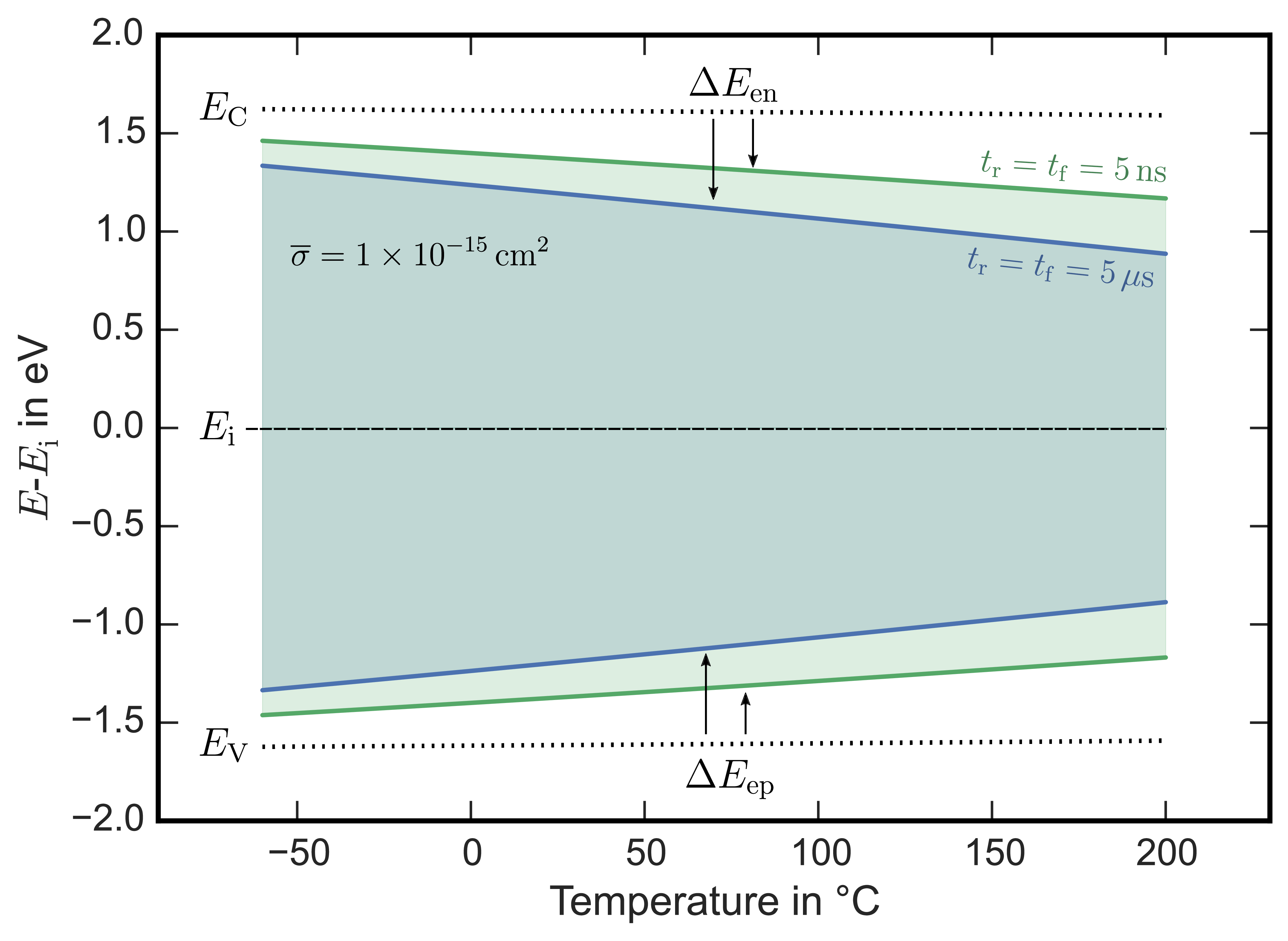
band gap. Fig. 1.18 shows the temperature dependence of between −60 °C and
200 °C for two fixed pulse slopes of
within a certain range of the semiconductors
band gap. Fig. 1.18 shows the temperature dependence of between −60 °C and
200 °C for two fixed pulse slopes of  and
and  .
.
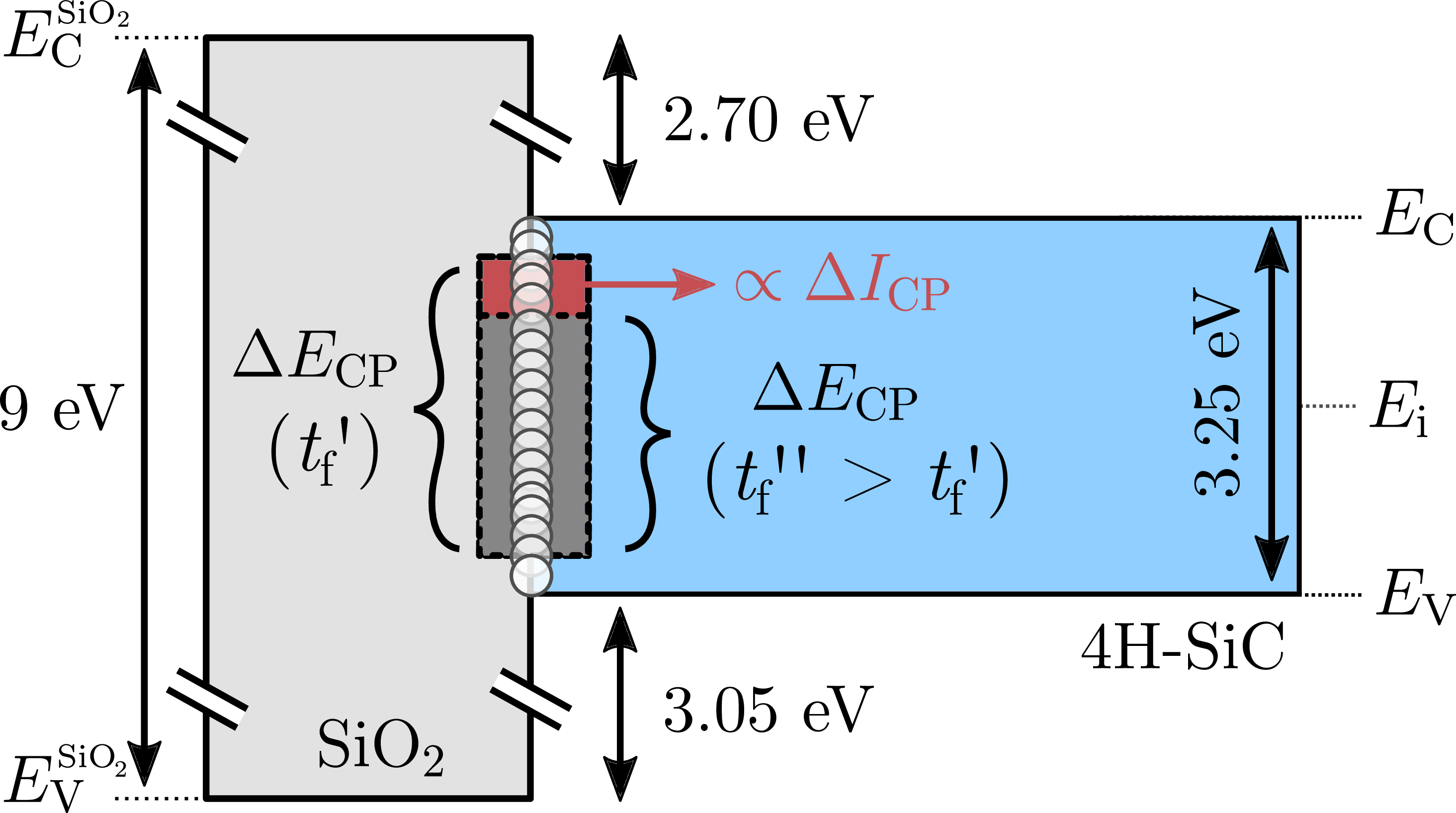


Fig. 1.19 illustrates, how this effect is used in spectroscopic CP to obtain the energetic distribution of the interface/border trap states in the upper half of the band gap. The same
formalism holds for the lower part of the band gap by replacing with . At a fixed and rise time , the charge pumping measurement is performed
two times with two different fall times  and
and  , with being the faster, and the slower one. For , is given by
  , whereas for the slower fall time
, the upper boundary of the active energy
window,
, whereas for the slower fall time
, the upper boundary of the active energy
window,  , is further away from the SiC conduction band
due to (1.13), which results in the narrower active energy window
, is further away from the SiC conduction band
due to (1.13), which results in the narrower active energy window  . Due to this, traps which are located within the energetic range

do not contribute to the charge pumping current in the measurement with . Therefore, the difference between both
charge pumping currents

is directly proportional to the within  . A spectroscopic scan along a large fraction of the SiC band gap is now easily
possible by varying , which moves the energetic position of along the band gap. Therefore, the energetic resolution of spectroscopic charge
pumping is given by , which also depends on but can be reduced by minimizing
. A spectroscopic scan along a large fraction of the SiC band gap is now easily
possible by varying , which moves the energetic position of along the band gap. Therefore, the energetic resolution of spectroscopic charge
pumping is given by , which also depends on but can be reduced by minimizing  according to (1.15).
1.3.5 Photo-assisted capacitance voltage profiling
Common techniques for the analysis of capacitance-voltage (CV) curves, like the high-frequency Terman method [90], do not work well in wide band gap semiconductors such as SiC [91]. The Terman technique is based on the
assumption that the interface states are not able to follow the small, high frequency AC signal, whereas they follow changes in the overlaying DC bias. For wide band gap semiconductors like SiC, this assumption leads to a significant
underestimation of the interface state density because deep states can not follow changes in the DC bias. For a measurement at room temperature and a very slow slew rate of 10 s/V the Terman technique can accurately
measure only between 0.2 eV and 0.6 eV above  , which is less than 15 % of the 4H-SiC
bandgap [91].
, which is less than 15 % of the 4H-SiC
bandgap [91].
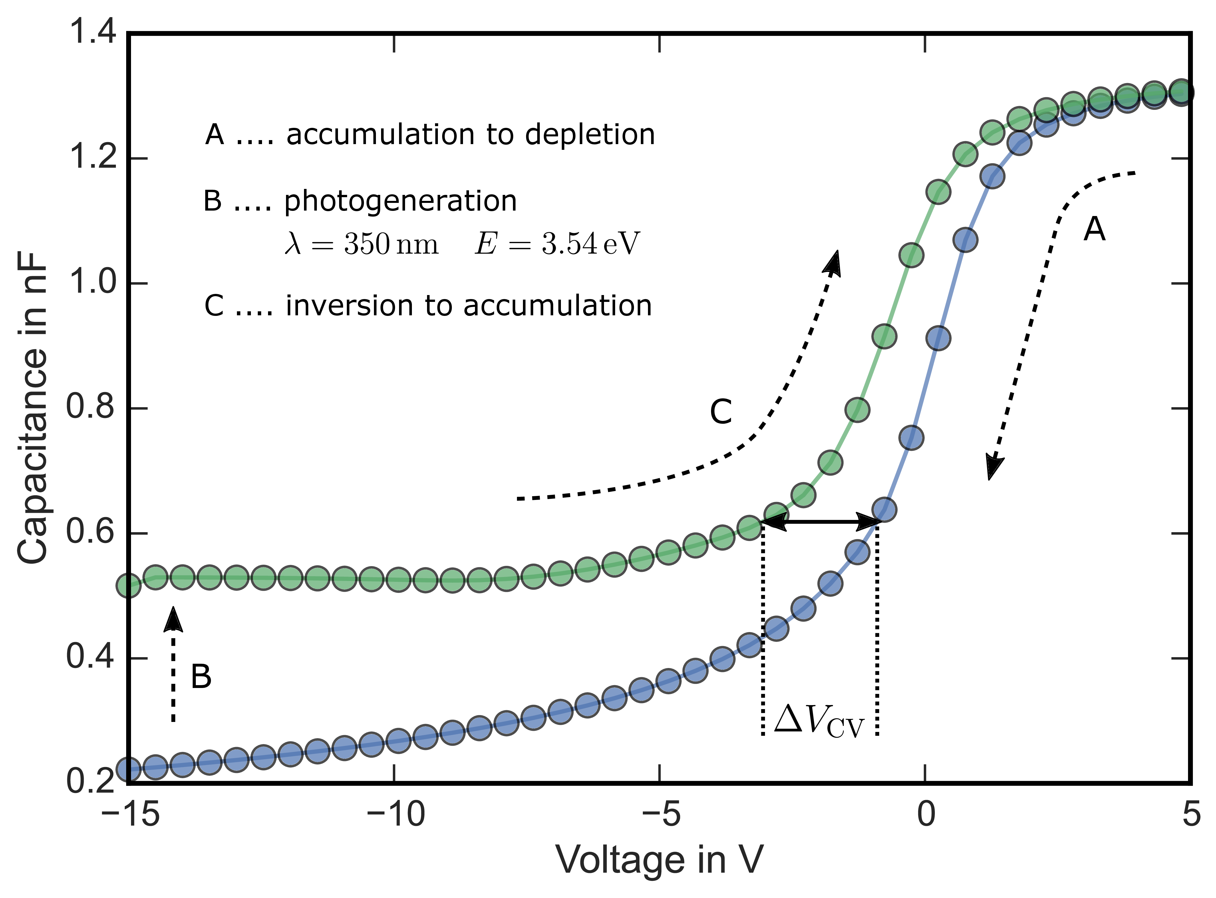
Figure 1.20: Photo-assisted CV measurement on an n-MOS capacitor. After the sweep from accumulation to depletion in the dark (A), the sample is illuminated with 350 nm light while the bias is kept at
−15 V. Due to the generation of minority carriers, and therefore the formation of an inversion layer, the capacitance increases (B). The hysteresis  , which occurs in the following sweep back to ac-
cumulation in the dark, can be used to estimate the density of interface/border traps.
, which occurs in the following sweep back to ac-
cumulation in the dark, can be used to estimate the density of interface/border traps.
A more promising and simpler to use method for a quick estimation of the number of interface/border states  across the band gap at room temperature is the
photo-assisted CV technique [92–96]. A typical photo-CV curve is illustrated in Fig. 1.20 for a n-type 4H-SiC MOS capacitor. The voltage is swept from accumulation to
deep depletion in the dark, which results in the blue curve (A). Due to the low thermal generation rate of minority carriers in wide band gap semiconductors like 4H-SiC, no inversion layer is formed within a reasonable amount of time
at room temperature. Therefore, the sample is illuminated with 350 nm (corresponding to 3.54 eV) light to populate the inversion layer via photogeneration while the bias is held at −15 V. The formation of
the inversion layer is visible as a rise in the capacitance towards an equilibrium value (B). After the inversion layer is fully formed, the light is turned off and the voltage is swept back to accumulation in the dark, which results in the
green curve (C). Here, a voltage shift occurs between both curves, which is caused by
minority carriers (in this case holes) trapped in interface states [97, 98]. The number of trapped states per cm2 can be estimated via
across the band gap at room temperature is the
photo-assisted CV technique [92–96]. A typical photo-CV curve is illustrated in Fig. 1.20 for a n-type 4H-SiC MOS capacitor. The voltage is swept from accumulation to
deep depletion in the dark, which results in the blue curve (A). Due to the low thermal generation rate of minority carriers in wide band gap semiconductors like 4H-SiC, no inversion layer is formed within a reasonable amount of time
at room temperature. Therefore, the sample is illuminated with 350 nm (corresponding to 3.54 eV) light to populate the inversion layer via photogeneration while the bias is held at −15 V. The formation of
the inversion layer is visible as a rise in the capacitance towards an equilibrium value (B). After the inversion layer is fully formed, the light is turned off and the voltage is swept back to accumulation in the dark, which results in the
green curve (C). Here, a voltage shift occurs between both curves, which is caused by
minority carriers (in this case holes) trapped in interface states [97, 98]. The number of trapped states per cm2 can be estimated via

Previous: 1.2 Detrimental Effects in MOS Devices Top: 1 Introduction Next: 2 On the first Component: the Subthreshold Hysteresis