« PreviousUpNext »Contents
Previous: 4.3 Analysis of minority carrier traps using photo-assisted CV Top: 4 Charge accumulation in high temperature processing steps Next: 4.5 Summary
4.4 Interpretation of the results
Although a change of the interface charging state after high temperature processing steps was expected before the study, the build up of such high amounts of positive fixed charges at the SiC/SiO2 interface is a
surprising outcome. Since the CV-curve after the initial high- step
step  is nearly identical to the ideal one, although the
thermal budget of is one of the highest, the deposition of the
polycrystalline gate contact
is nearly identical to the ideal one, although the
thermal budget of is one of the highest, the deposition of the
polycrystalline gate contact  seems of fundamental importance for the involved
mechanism.
seems of fundamental importance for the involved
mechanism.
4.4.1 Charge accumulation via impurity diffusion
A first possibility is that (poly-deposition) might add impurities, like mobile
ions with low diffusion constants at room temperature, to the system. However, these mobile ions could have been present in the system already before . In this case, a voltage shift arises after due to the deposited gate contact, which introduces
an electric field along the oxide layer due to the alignment of the Fermi levels. The mechanism is explained schematically in Fig. 4.9. After , the system is in thermal equilibrium and no
electric field is present along the SiO2 (left). Subsequently to , an oxide field  arises due to the Fermi-level alignment.
Therefore, positive mobile ions are able to diffuse along the direction of to the SiC/SiO2 interface due to
the very high processing temperatures. In the end, this leads to an accumulation of fixed positive charges at the SiC/SiO2 interface. It is furthermore important to note that, likely due to diffusion quenching at low
temperatures, it was not possible to move these trapped charges away from the interface (recover the CV curve to its ideal position) via a gate stress bias, even at elevated measurement temperatures of up to 200 °C.
arises due to the Fermi-level alignment.
Therefore, positive mobile ions are able to diffuse along the direction of to the SiC/SiO2 interface due to
the very high processing temperatures. In the end, this leads to an accumulation of fixed positive charges at the SiC/SiO2 interface. It is furthermore important to note that, likely due to diffusion quenching at low
temperatures, it was not possible to move these trapped charges away from the interface (recover the CV curve to its ideal position) via a gate stress bias, even at elevated measurement temperatures of up to 200 °C.

Figure 4.9: Top: schematic band alignment during a high-temperature processing step. After , the system consists of the semiconductor with the
oxide layer on top. Therefore, no electric field is present in the SiO2 layer (left). In
all following processing steps  , the silicon gate contact introduces an electric field
in the oxide layer due to the Fermi level alignment (right). In combination with the high temperatures of several hundred Celsius, positive charges are now able to diffuse to the SiC/SiO2 interface through the oxide layer,
which leads to a build-up of positive charges at the interface. Bottom: schematic cross section indicating the accumulation of positive charges at the SiC/SiO2 interface.
, the silicon gate contact introduces an electric field
in the oxide layer due to the Fermi level alignment (right). In combination with the high temperatures of several hundred Celsius, positive charges are now able to diffuse to the SiC/SiO2 interface through the oxide layer,
which leads to a build-up of positive charges at the interface. Bottom: schematic cross section indicating the accumulation of positive charges at the SiC/SiO2 interface.
4.4.2 Hydrogen related charge accumulation
In addition to the previously discussed mobile ion mechanism, another possible explanation can be given using a hydrogen-based mechanism like the hydrogen-release model, which was described in Section 1.2.2. A simplified picture of the mechanism, which might lead to the observed charge accumulation, is shown in Fig. 4.10. During , the Tetraethylorthosilicat (TEOS) based
SiO2 film, which was deposited via chemical vapor deposition (CVD), is annealed in an inert dinitrogen (N2) atmosphere at a temperature above 1000 °C for the time  . Due to the highly
elevated temperature and the inert atmosphere, which results in a low H partial pressure in the chamber, trapped and residual hydrogen is likely to be released from the amorphous SiO2 (Fig. 4.10, top, left). Therefore, no significant deviation of the CV curve from the ideal one should be observed after , which is indeed the case as was shown above using
the simulated CV curves. After (POA),
. Due to the highly
elevated temperature and the inert atmosphere, which results in a low H partial pressure in the chamber, trapped and residual hydrogen is likely to be released from the amorphous SiO2 (Fig. 4.10, top, left). Therefore, no significant deviation of the CV curve from the ideal one should be observed after , which is indeed the case as was shown above using
the simulated CV curves. After (POA),  remains at approximately
1 × 10⁹/cm2, which results in a
remains at approximately
1 × 10⁹/cm2, which results in a  close to the ideal flatband voltage (compare
with Fig. 4.8, POA).
close to the ideal flatband voltage (compare
with Fig. 4.8, POA).
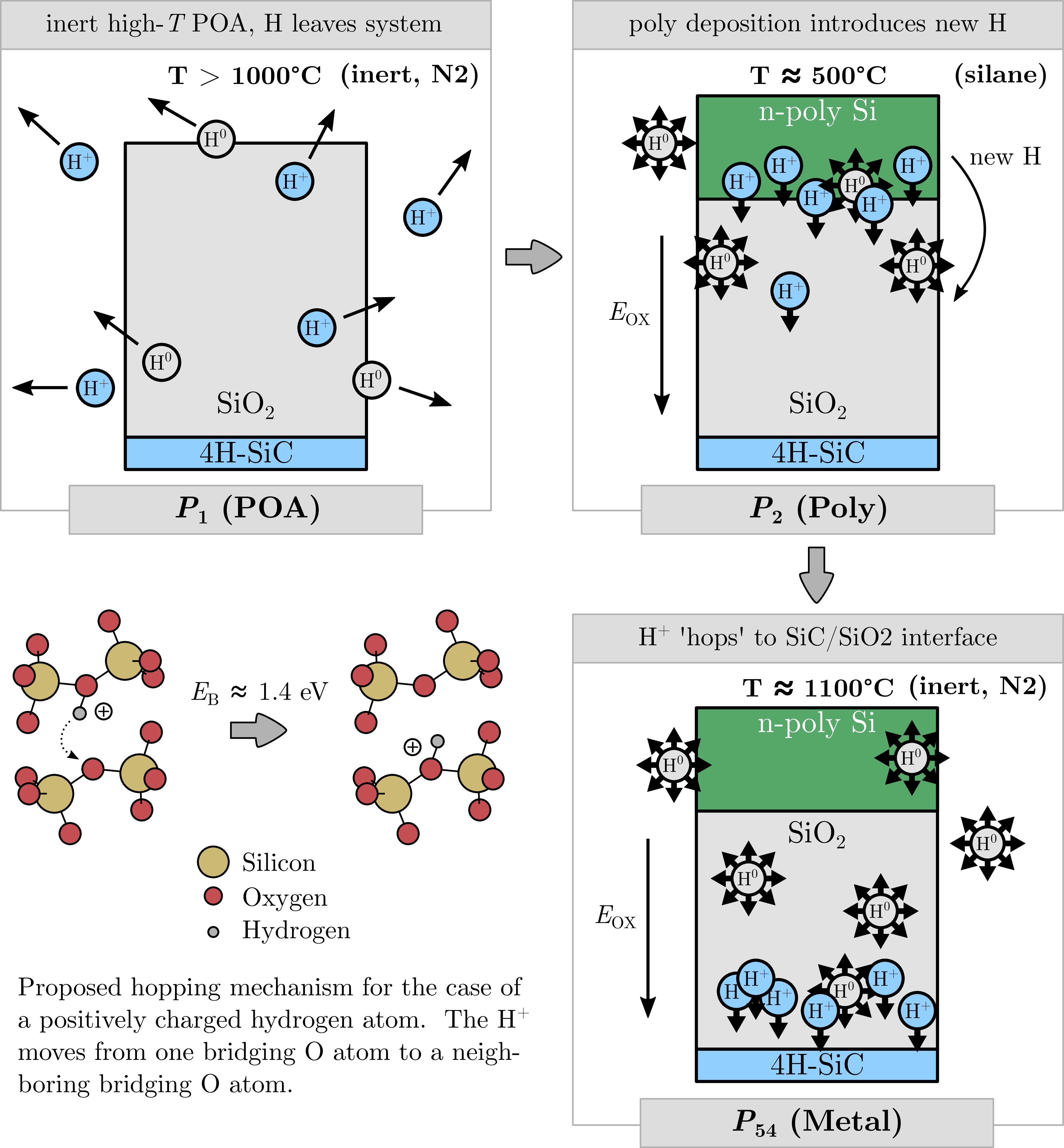
Figure 4.10: Proposed mechanism of positive charge accumulation at the SiO2/SiC interface using a hydrogen based model. Top, left: during the post oxidation anneal (), H is removed from the SiO2/SiC stack
due to the high thermal budget and the inert gas composition in the chamber. Top, right: The deposition of the polycrystalline silicon gate introduces high amounts of H into the system. Furthermore, the positively charged hydrogen,
 , is strongly affected by the oxide field, which results from the difference
in work-functions of the poly-Si gate and 4H-SiC. Bottom, right: positively charged H is pushed in the direction of , which leads to a build-up of at the SiC/SiO2 interface and a significant shift of to more negative voltages. On the other hand,
, is strongly affected by the oxide field, which results from the difference
in work-functions of the poly-Si gate and 4H-SiC. Bottom, right: positively charged H is pushed in the direction of , which leads to a build-up of at the SiC/SiO2 interface and a significant shift of to more negative voltages. On the other hand,
 does not move in a preferred direction due to the neutral charge state.
Bottom, left: possible mechanism of hydrogen hopping. binds to a bringing oxygen atom and is able to hop to a bringing
oxygen atom in the vicinity by overcoming an energy barrier of approximately
does not move in a preferred direction due to the neutral charge state.
Bottom, left: possible mechanism of hydrogen hopping. binds to a bringing oxygen atom and is able to hop to a bringing
oxygen atom in the vicinity by overcoming an energy barrier of approximately  [58] resulting
in a drift of bound to the SiC/SiO2 interface.
[58] resulting
in a drift of bound to the SiC/SiO2 interface.
The amount of available hydrogen in the system changes drastically after the deposition of the polycrystalline silicon gate in the process step (Fig. 4.10, top right). Here, the poly-Si gate is grown by chemical decomposition of silane (SiH4) at a temperature slightly above 500 °C, which
releases enormous amounts of hydrogen via pyrolysis. Additionally, also the SiO2 film is flooded again with neutral and positively charged protons . Furthermore, the alignment of the Fermi levels results in an electric
field along the oxide layer between the poly-Si metal
gate and the semiconductor, which points in the direction of the SiC/SiO2 interface, as already discussed in the previous section. Due to its neutral charge, will not be affected by , which results in a random movement of through the material (indicated via the arrows). On the other hand,
the positive charge state, , is strongly affected by resulting in a preferred direction of the
hydrogen migration along the electric field, which points in the direction of the SiC/SiO2 interface. The hydrogen migration process will continue in each additional high temperature manufacturing step, which in the end
results in a high amount of positive charges trapped at the SiC/SiO2 interface (Fig. 4.10, bottom right). In addition to the drift of the positive
hydrogen, the neutral hydrogen may occupy a trapping site close to the channel and capture a hole,
thereby creating additional positive charges [58]. The accumulation of is visible in the CV curves as a significant shift of to more negative voltages.
As discussed in Section 1.10, interstitial hydrogen, either in the positive or neutral configuration, will easily bind to several precursors in the
amorphous SiO2 with a low energy barrier of  [58]. Therefore,
hydrogen diffusion in the dielectric seems to be limited. However, H bonded to a bridging oxygen atom is able to "hop" from one bound state to the next bound state by overcoming a barrier of approximately as depicted
in Fig. 4.10 (bottom, left), which likely results in an additional specific temperature dependence of the observed charge accumulation mechanism.
[58]. Therefore,
hydrogen diffusion in the dielectric seems to be limited. However, H bonded to a bridging oxygen atom is able to "hop" from one bound state to the next bound state by overcoming a barrier of approximately as depicted
in Fig. 4.10 (bottom, left), which likely results in an additional specific temperature dependence of the observed charge accumulation mechanism.
In the next section, it will be shown that the extracted activation energy of the observed charge accumulation mechanism during high temperature processing steps is in the range of proposed energy barriers for hydrogen-related models [48, 58, 132].
Barrier extraction
For the extraction of the energy barrier  , we assume the diffusivity of hydrogen in the
the amorphous SiO2 is not rate limiting [70], and the underlying mechanism is related to hydrogen release (see Section 1.9), which is of
course speculative. It is important to note that the knowledge of the exact atomistic mechanism is not necessary for the energy barrier extraction. Therefore, the hydrogen release mechanism is only exemplary. In reality, there might
be numberless candidates, which qualify according to the extracted energy barrier.
, we assume the diffusivity of hydrogen in the
the amorphous SiO2 is not rate limiting [70], and the underlying mechanism is related to hydrogen release (see Section 1.9), which is of
course speculative. It is important to note that the knowledge of the exact atomistic mechanism is not necessary for the energy barrier extraction. Therefore, the hydrogen release mechanism is only exemplary. In reality, there might
be numberless candidates, which qualify according to the extracted energy barrier.
For a normally distributed , the release of from the bound state to the interstitial state, should also be
distributed in time with a specific time constant  for each transition event. Here, obeys the Maxwell–Boltzmann statistics
according to
for each transition event. Here, obeys the Maxwell–Boltzmann statistics
according to

with the Boltzmann constant  , the temperature and the pre-exponential factor
  .
.
The energy barrier which has to be overcome to enable the
accumulation of positive charges at the SiC/SiO2 interface, was extracted by using a fit of the flatband voltage shift  as a function of the time
  , for which the sample was subjected to a high
temperature. For a normally distributed , has to obey
, for which the sample was subjected to a high
temperature. For a normally distributed , has to obey

with the error function erfc, which is given in (1.5), the mean value,  , and the standard deviation
  , of the normally distributed , and the maximum flatband voltage shift
  as an additional fitting parameter.
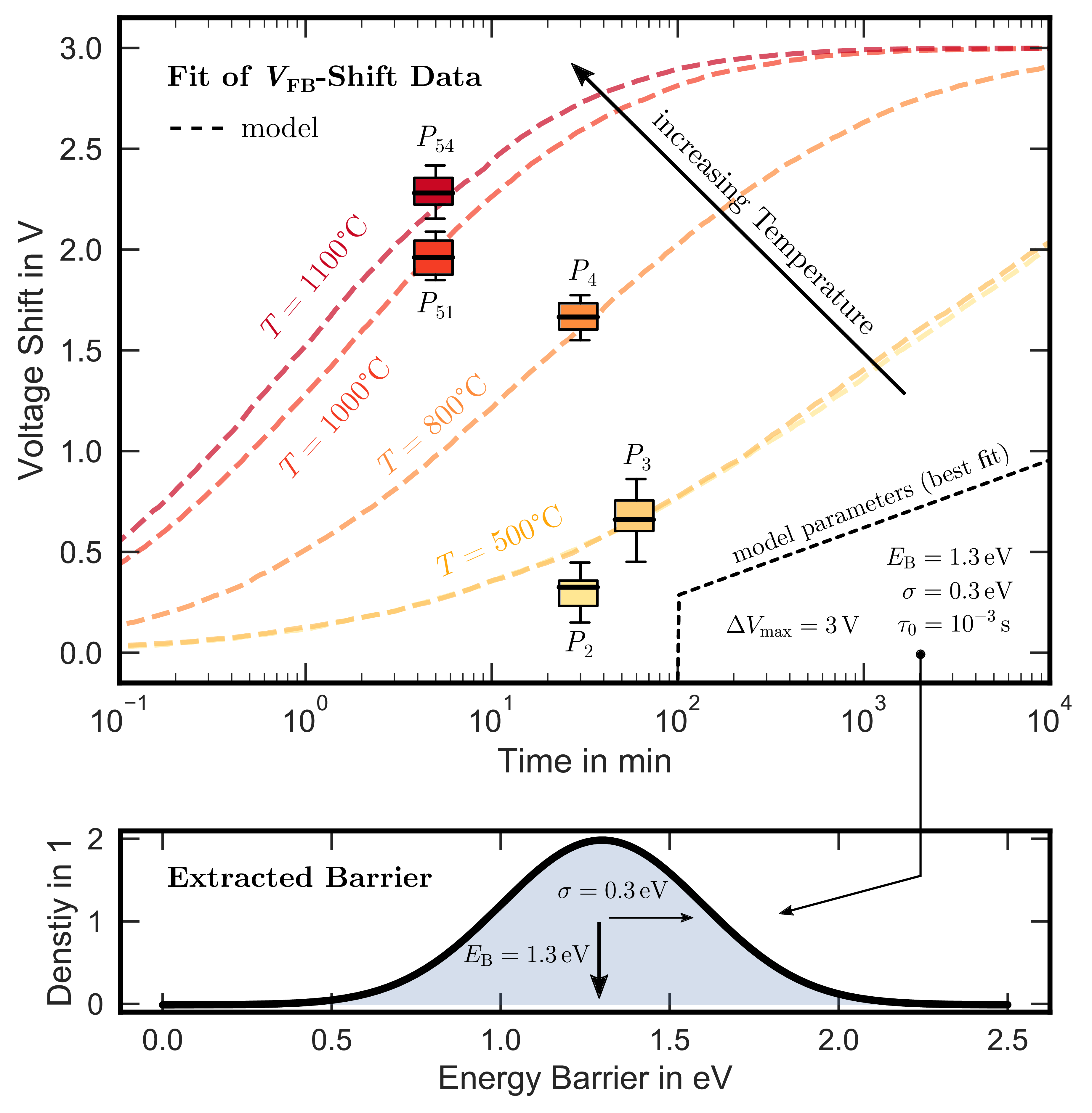
Figure 4.11: Fit of the flatband voltage shift as a function of the time at a given high temperature processing step. The boxes represent the flat band voltage shift after the processing steps (Poly),  (ILD),
  (Anneal),
  and (metal contact). Dashed lines represent a fit ac-
cording to (4.2), assuming a normally distributed energy barrier . The extracted fitting parameters are given in
the inset. The data shows good agreement with an underlying transition mechanism with a mean energy barrier of
and (metal contact). Dashed lines represent a fit ac-
cording to (4.2), assuming a normally distributed energy barrier . The extracted fitting parameters are given in
the inset. The data shows good agreement with an underlying transition mechanism with a mean energy barrier of  and a standard de-
viation of
and a standard de-
viation of  . The extracted dis-
tribution of the energy barrier is shown in the bottom plot.
. The extracted dis-
tribution of the energy barrier is shown in the bottom plot.
Fig. 4.11 shows a fit of the data from Fig. 4.3 for the barrier extraction. The boxes represent the flat band voltage shift after the processing steps (Poly), (ILD), (Anneal), and (metal contact). The dashed lines represent the
fit according to (4.2) for the representative process temperatures ranging from 500 °C for and (yellow), to 1100 °C for the metal
contact formation  (red). The fitting parameters are given in the
inset. The transition barrier for the mechanism, which results in the observed , is approximately
(red). The fitting parameters are given in the
inset. The transition barrier for the mechanism, which results in the observed , is approximately  (Fig. 4.11, bottom), which is in good agreement with proposed energy barriers for the hydrogen release model [48, 58, 132, 133]. A comparison of energy barriers proposed by
DFT simulations for various hydrogen related transition events and extracted in this work from the thermal budget
data via the fit in Fig. 4.11 (experimental) is provided in Tab. 4.2.
(Fig. 4.11, bottom), which is in good agreement with proposed energy barriers for the hydrogen release model [48, 58, 132, 133]. A comparison of energy barriers proposed by
DFT simulations for various hydrogen related transition events and extracted in this work from the thermal budget
data via the fit in Fig. 4.11 (experimental) is provided in Tab. 4.2.
Table 4.2: Comparison of energy barriers proposed by DFT simulations for various hydrogen related transition events [48, 58, 132, 133] and extracted from the thermal budget data via the
fit in Fig. 4.11 (experimental). The extracted energy barrier shows good agreement with hydrogen-related models, which provides a possible explanation for the observed
charge accumulation via a build-up of positively charged H at the SiC/SiO2 interface.
| Type | |
 |
| experimental | 1.30 | 0.30 |
| release of from bridging O (DFT) |
1.50 | 0.30 |
| hopping of from bridging O (DFT) |
1.55 | 0.60 |
| hopping of from bridging O (DFT) |
1.40 | 0.75 |
Previous: 4.3 Analysis of minority carrier traps using photo-assisted CV Top: 4 Charge accumulation in high temperature processing steps Next: 4.5 Summary