« PreviousUpNext »Contents
Previous: 4 Charge accumulation in high temperature processing steps Top: 4 Charge accumulation in high temperature processing steps Next: 4.3 Analysis of minority carrier traps using photo-assisted CV
4.2 Evolution of fixed oxide charges
Fig. 4.2 shows the normalized CV curves after each high temperature processing step given in Tab. 4.1 for 5 n-MOSCAPs from each sample group (wafer). All CV measurement were performed at 30 °C and a frequency of 100 kHz from depletion at −15 V to accumulation at 15 V (up-sweep) and vice versa (down-sweep). With increasing thermal budget, the CV curves shift to more negative voltages. The voltage shift is parallel, which indicates a build-up of fixed positive charges at the SiC/SiO2 interface. It is important to note that the observed voltage shift is in fact due to the high thermal budget and not caused by the direction of the CV measurement, due to the negligible difference for both sweep directions (not shown).


The flatband voltage  extracted from the up- and down- sweep in the
data at an extraction level of
extracted from the up- and down- sweep in the
data at an extraction level of  (dotted line) is depicted
in Fig. 4.3. Although
(dotted line) is depicted
in Fig. 4.3. Although  is one of the steps with the highest thermal budget
(
is one of the steps with the highest thermal budget
( for
for  ), the CV curve
remains close to the theoretical one (as will be shown in Section 4.2.1). The first shift of the CV curve occurs after
), the CV curve
remains close to the theoretical one (as will be shown in Section 4.2.1). The first shift of the CV curve occurs after  , which is the deposition of the polysilicon gate. At
this point, has already shifted by 300 mV. The
voltage shift increases with each additional high-
, which is the deposition of the polysilicon gate. At
this point, has already shifted by 300 mV. The
voltage shift increases with each additional high- processing step to a maximum
  of approximately 2.35 V after
  . Furthermore, it is important to note that the
impact of the gate bias on is negligible (
. Furthermore, it is important to note that the
impact of the gate bias on is negligible ( ) compared to the overall
voltage shift, which arises due to the thermal budget.
) compared to the overall
voltage shift, which arises due to the thermal budget.
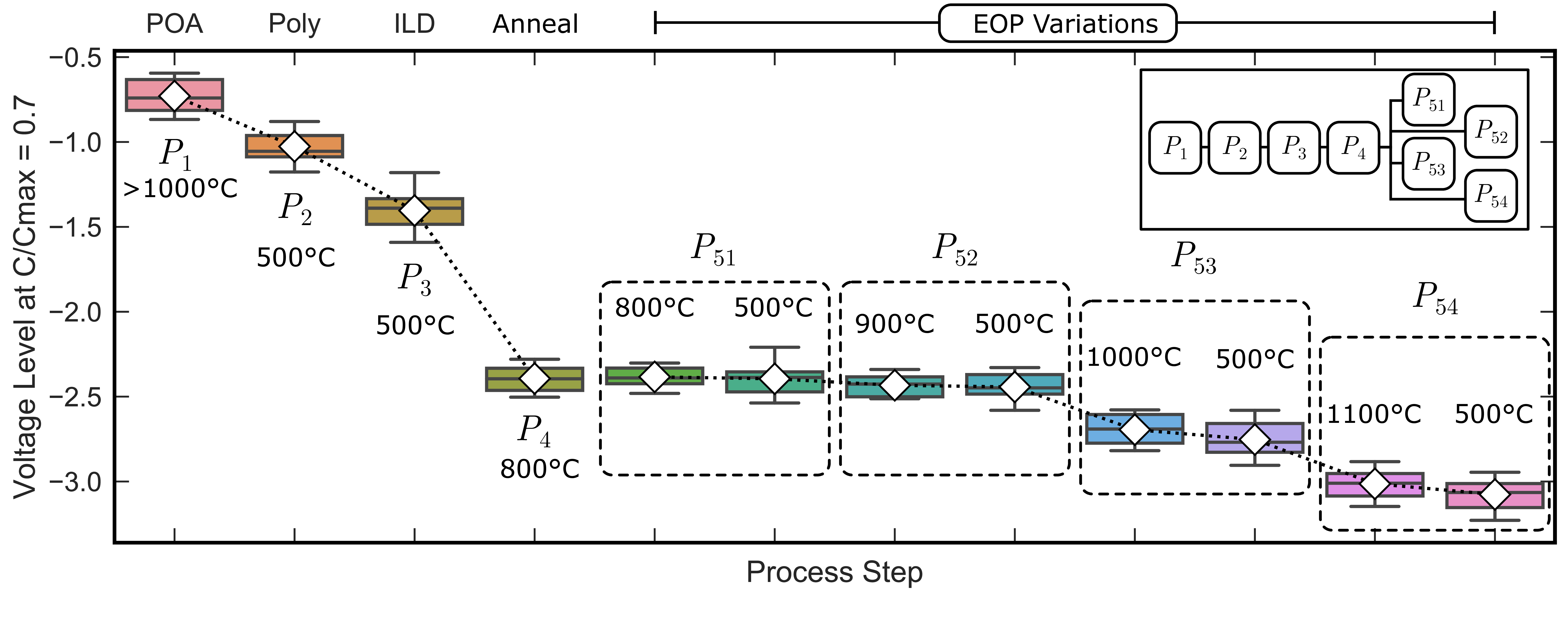
Figure 4.3: Flatband voltage after all high-temperature processing steps.  was extracted at the dashed line in Fig. 4.2.
arises after the deposition of the poly-Si gate con-
tact and increases with each additional processing step with a high thermal budget.
was extracted at the dashed line in Fig. 4.2.
arises after the deposition of the poly-Si gate con-
tact and increases with each additional processing step with a high thermal budget.
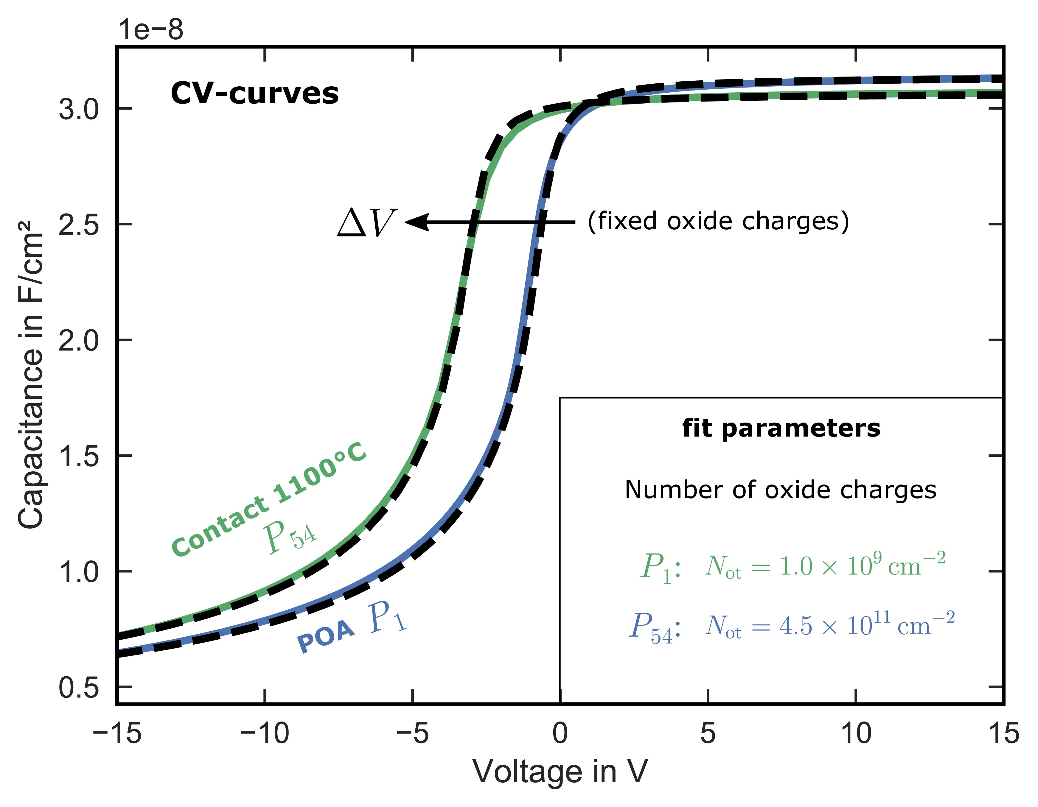
Figure 4.4: Measured CV-curves after the first (POA, ) and the last (Contact 1100 °C, ) high- processing step. The CV curve of is shifted to more negative gate voltages due to
the high thermal budget, which led to a build-up of positive oxide charges. Both curves have been simulated using a total number of oxide charges of 1.0 × 10⁹/cm2 for and 4.5 × 10¹¹/cm2 for
.  was set to 1.0 × 10⁹/(cm2 eV)
for both curves.
was set to 1.0 × 10⁹/(cm2 eV)
for both curves.
4.2.1 Simulated CV curves
Fig. 4.4 shows a comparison of the measured CV curves after (blue) and (green), which did show the highest shift, with a
simulated CV signal (dashed) of the poly-Si/SiO2/SiC MOS-System. After , the CV curve is very similar to the ideal curve of
the system with a total number of oxide traps  of approximately
1 × 10⁹/cm2 (blue). After the last processing step, , is shifted to more negative gate voltages due to
an increase in trapped positive charges. For the fit, a of approximately
of approximately
1 × 10⁹/cm2 (blue). After the last processing step, , is shifted to more negative gate voltages due to
an increase in trapped positive charges. For the fit, a of approximately  (green)
results in a good agreement with the experimental data. Fig. 4.5 shows the values extracted from the fitting parameters for the complete set of high- processing steps.
(green)
results in a good agreement with the experimental data. Fig. 4.5 shows the values extracted from the fitting parameters for the complete set of high- processing steps.
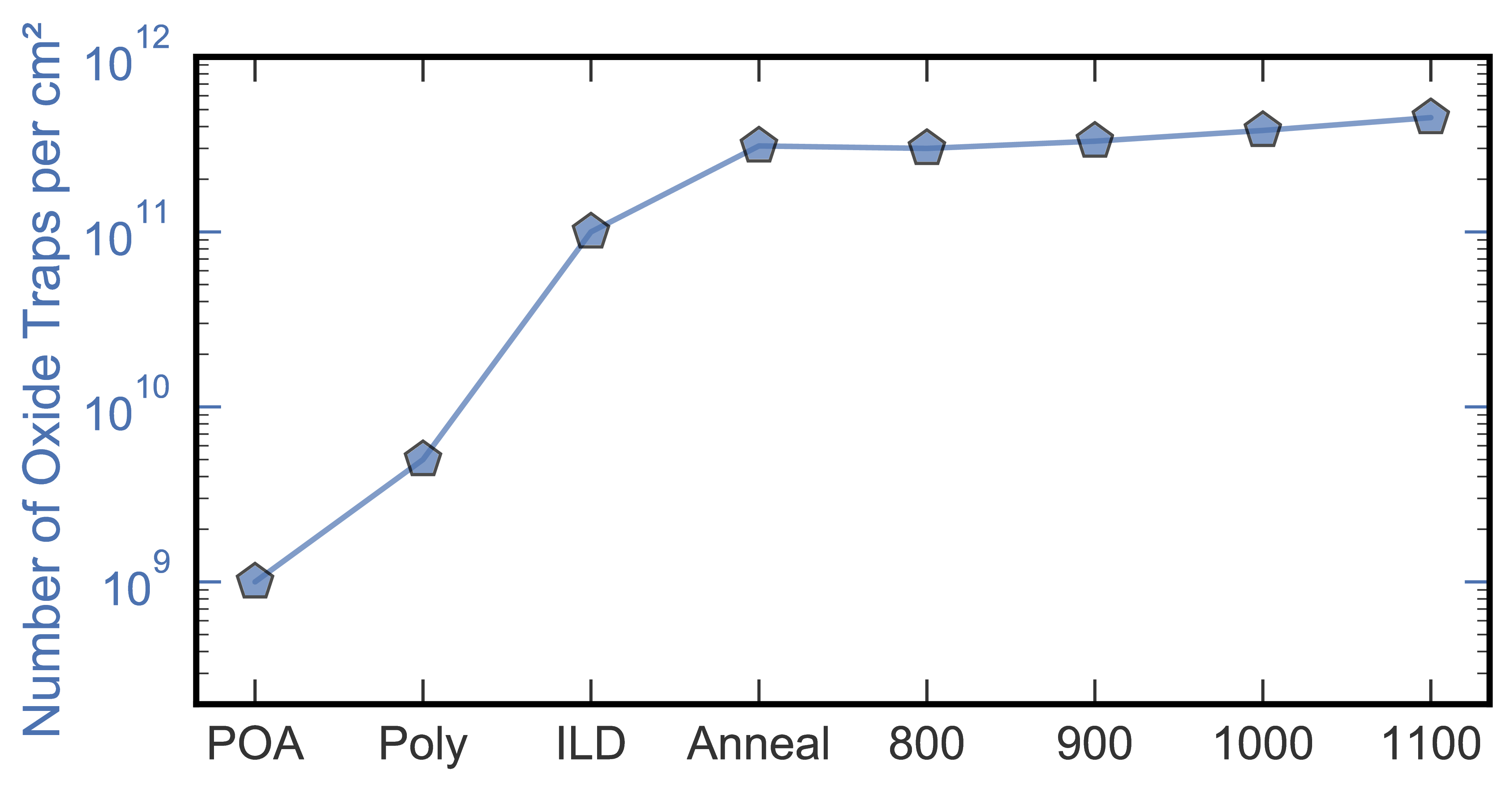
Figure 4.5: Number of positive oxide charges after each high temperature processing step. Af-
ter the poly-Si deposition , increases strongly from 1.0 × 10⁹/cm2
up to 4.5 × 10¹¹/cm2 after  assuming all charges at the SiC/SiO2
interface. The high corresponds to a maximum flatband voltage shift
of approximately 2.3 V.
assuming all charges at the SiC/SiO2
interface. The high corresponds to a maximum flatband voltage shift
of approximately 2.3 V.
Previous: 4 Charge accumulation in high temperature processing steps Top: 4 Charge accumulation in high temperature processing steps Next: 4.3 Analysis of minority carrier traps using photo-assisted CV