« PreviousUpNext »Contents
Previous: 3.2 Similarities in BTI of commercially available SiC-power MOSFETs Top: 3 On the second Component: Bias Temperature Instability Next: 4 Charge accumulation in high temperature processing steps
3.3 Preconditioned BTI measurements
This section focuses on various  extraction techniques after positive bias stress. It will be demonstrated that most
of the voltage shift typically observed in standardized measurement tests (e.g. JEDEC-like) on
4H-SiC devices results from erroneous extraction techniques including stress independent but fully reversible components, which do not degrade the device performance under regular dynamic operation. A new drift evaluation
technique based on device preconditioning before each readout is presented which allows for a more comprehensive and nearly
measurement delay- and recovery time independent determination of the permanent voltage shift component
extraction techniques after positive bias stress. It will be demonstrated that most
of the voltage shift typically observed in standardized measurement tests (e.g. JEDEC-like) on
4H-SiC devices results from erroneous extraction techniques including stress independent but fully reversible components, which do not degrade the device performance under regular dynamic operation. A new drift evaluation
technique based on device preconditioning before each readout is presented which allows for a more comprehensive and nearly
measurement delay- and recovery time independent determination of the permanent voltage shift component  . This component emerges after AC and
DC stress and is of fundamental importance from an application perspective.
. This component emerges after AC and
DC stress and is of fundamental importance from an application perspective.
3.3.1 The impact of thermal non-equilibrium during the reference readout
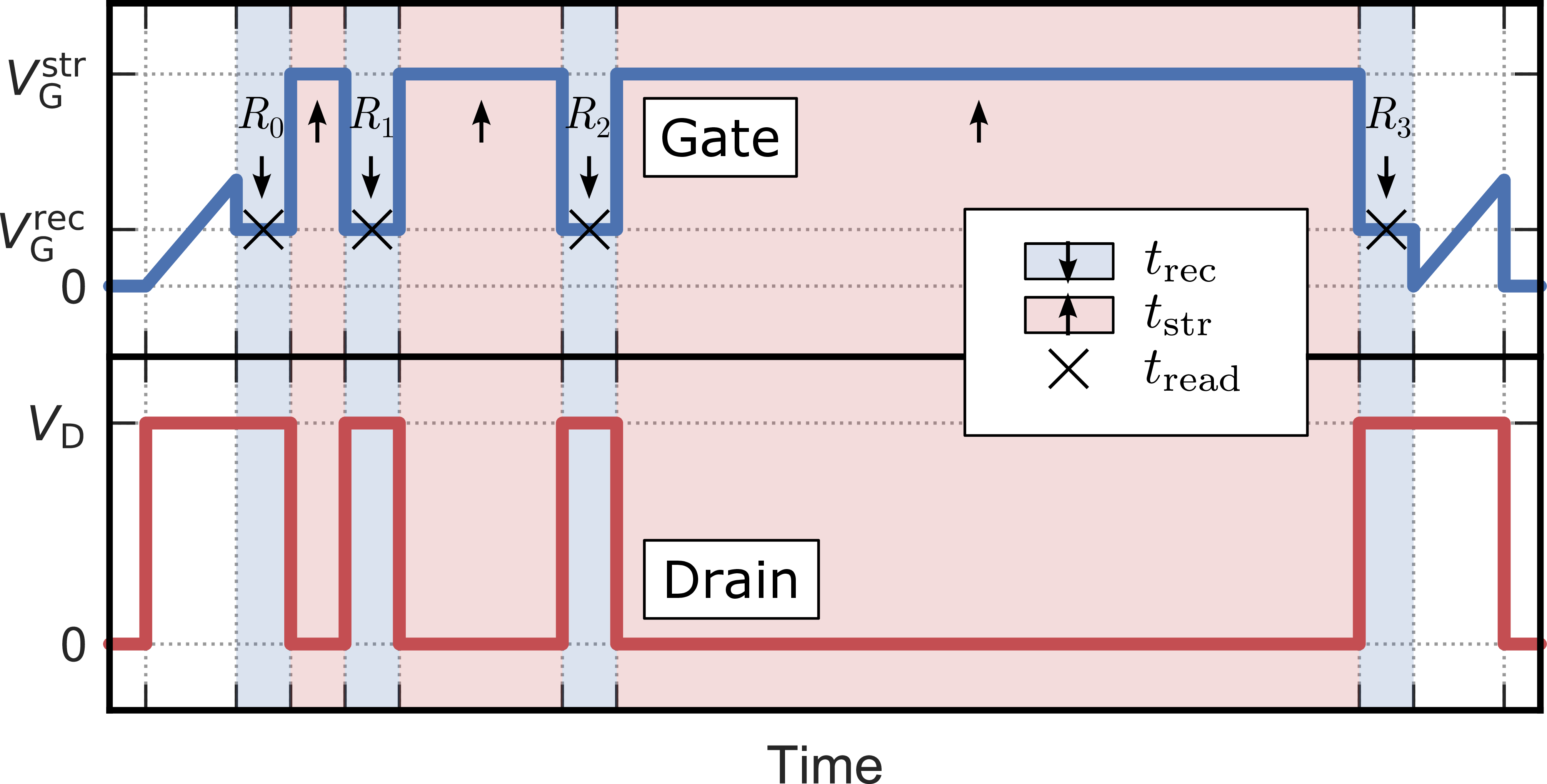
A BTI measurement test according to JEDEC standard JESD 241 [129] is shown in Fig. 3.7. The measurement pattern consists of a  sweep from 0 V to the maximum sweep
voltage
sweep from 0 V to the maximum sweep
voltage  for the calculation of the voltage shift followed
by a repeated readout cycle at the recovery voltage
for the calculation of the voltage shift followed
by a repeated readout cycle at the recovery voltage  in sequence with a stress cycle at the stress
voltage
in sequence with a stress cycle at the stress
voltage  with logarithmically increasing stress times
 . The drain voltage
  is turned off during every stress cycle to
suppress device heating, non-uniform electric oxide fields and hot-carrier degradation. After each stress pulse, the voltage shift is calculated from the recovery drain current with respect to the reference drain
current at the initial readout cycle (marked with
is turned off during every stress cycle to
suppress device heating, non-uniform electric oxide fields and hot-carrier degradation. After each stress pulse, the voltage shift is calculated from the recovery drain current with respect to the reference drain
current at the initial readout cycle (marked with  ). The drain current at each subsequent readout
cycle
). The drain current at each subsequent readout
cycle  is extracted at
  after the end of
the stress pulse. The resulting voltage shift is shown in Fig. 3.8 (JED, blue) after application of a stress voltage equal to two times the operation voltage
after the end of
the stress pulse. The resulting voltage shift is shown in Fig. 3.8 (JED, blue) after application of a stress voltage equal to two times the operation voltage  for stress times up to 1444 s at
30 °C. Using JESD 241, a voltage shift of 400 mV after 1444 s stress is recorded. A slightly changed
but common variation of the JESD 241 standard measurement is shown in Fig. 3.9. The pattern is similar to the pattern sketched in Fig. 3.7 with one small deviation: we introduce a 10 s delay at
for stress times up to 1444 s at
30 °C. Using JESD 241, a voltage shift of 400 mV after 1444 s stress is recorded. A slightly changed
but common variation of the JESD 241 standard measurement is shown in Fig. 3.9. The pattern is similar to the pattern sketched in Fig. 3.7 with one small deviation: we introduce a 10 s delay at  before the reference readout
to represent the influence of the often ill-defined
measurement delay. Although at first glance this modification appears to be negligible, the influence on the extracted voltage shift is significant as can be seen in Fig. 3.8 (JED0, green). While the trend over time does not change, an offset of approximately
before the reference readout
to represent the influence of the often ill-defined
measurement delay. Although at first glance this modification appears to be negligible, the influence on the extracted voltage shift is significant as can be seen in Fig. 3.8 (JED0, green). While the trend over time does not change, an offset of approximately  is introduced which
is merely due to changing the bias value prior to the reference readout .
is introduced which
is merely due to changing the bias value prior to the reference readout .
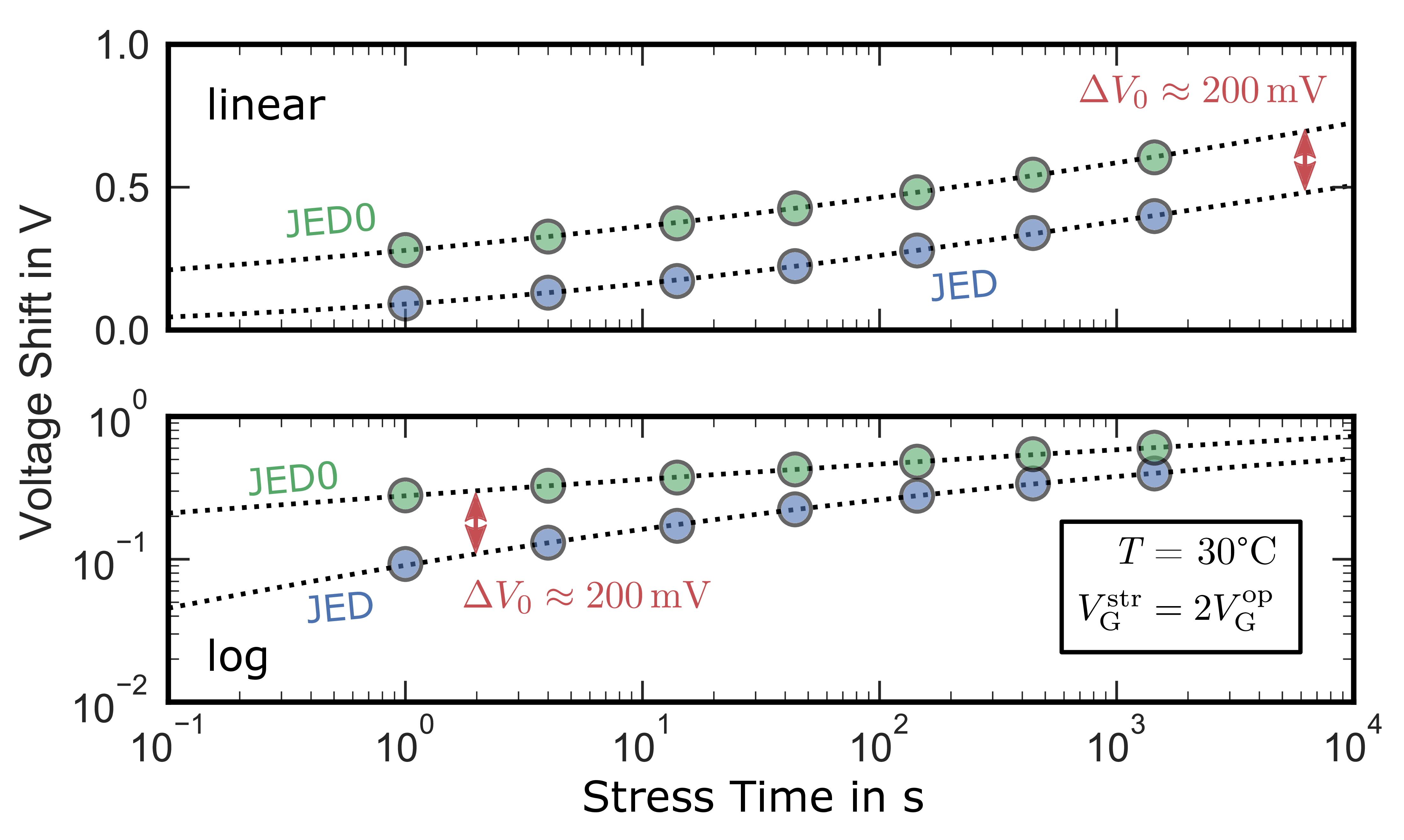
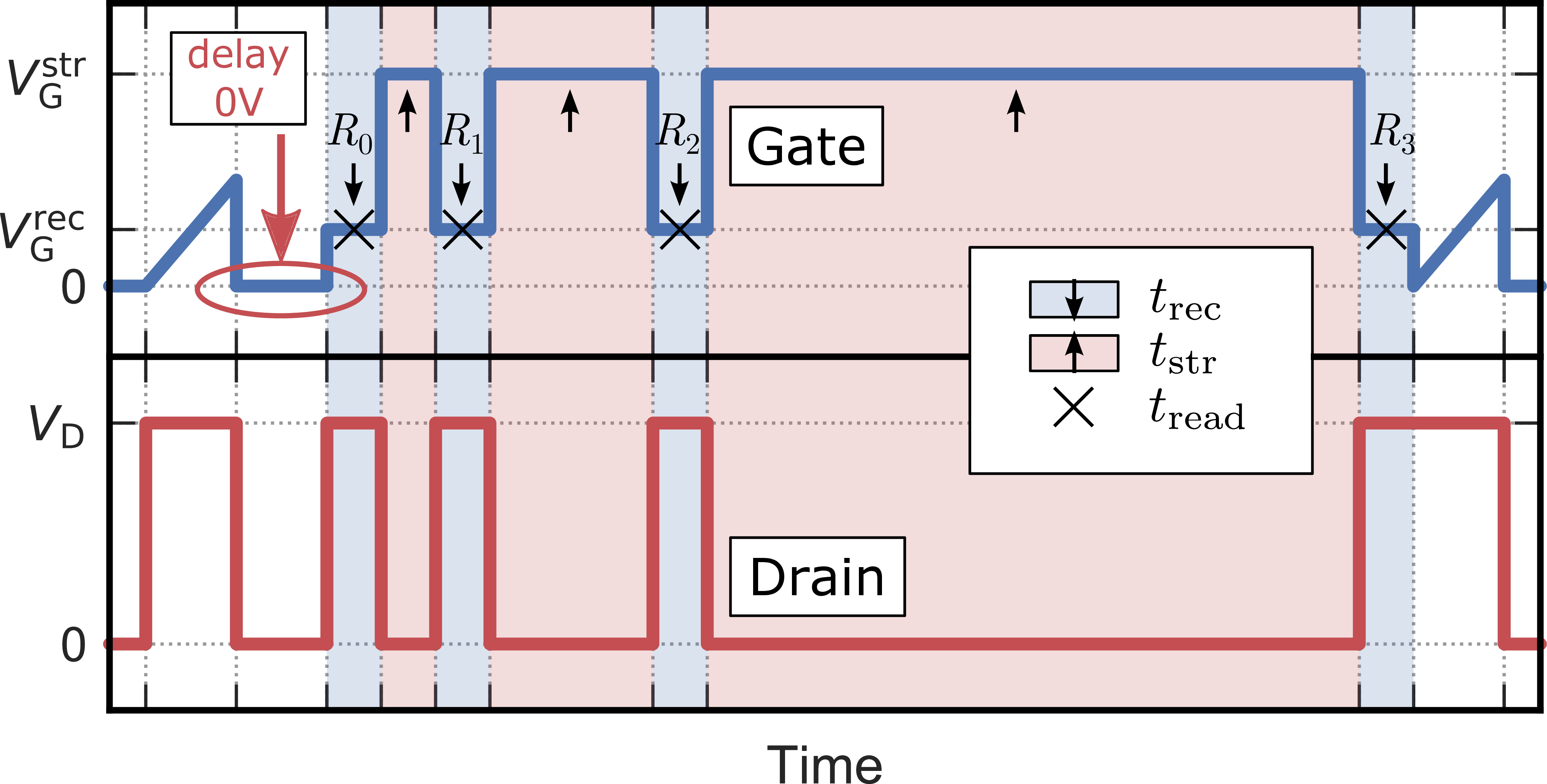
Figure 3.9: Delayed BTI measurement pattern (JED0) similar to JEDEC JESD 241 (Fig. 3.7), but with a delay at  before the reference readout .
The offset  results from the fact that the reference readout
strongly depends on the device bias history. Fig.
3.10 shows
results from the fact that the reference readout
strongly depends on the device bias history. Fig.
3.10 shows  at (
at ( ) for both measurement
patterns. The blue curve represents the measurement pattern according to JEDEC JESD 241 (JED), whereas the green curve represents the same pattern with a 10 s delay at before (referenced to as JED0). For JED, we observe
increasing drain current after the bias change from the end-of-sweep voltage to the readout voltage , indicating recovery of trapped electrons, which
where captured at
) for both measurement
patterns. The blue curve represents the measurement pattern according to JEDEC JESD 241 (JED), whereas the green curve represents the same pattern with a 10 s delay at before (referenced to as JED0). For JED, we observe
increasing drain current after the bias change from the end-of-sweep voltage to the readout voltage , indicating recovery of trapped electrons, which
where captured at  during the preceding
voltage sweep. The opposite trend is observed for JED0 (green). At the same readout voltage, JED0 shows a higher and decreasing drain current resulting from carrier trapping in oxide/border traps.
during the preceding
voltage sweep. The opposite trend is observed for JED0 (green). At the same readout voltage, JED0 shows a higher and decreasing drain current resulting from carrier trapping in oxide/border traps.
We therefore conclude that the discrepancy in at is due to the amount of time the system needs to
reach thermal equilibrium at a certain gate voltage, meaning every trap state with an energetic position below the Fermi level  is filled with electrons and every trap state
above is empty. Especially in wide band gap
semiconductors like silicon carbide, it may take a long time to reach thermal equilibrium.
is filled with electrons and every trap state
above is empty. Especially in wide band gap
semiconductors like silicon carbide, it may take a long time to reach thermal equilibrium.
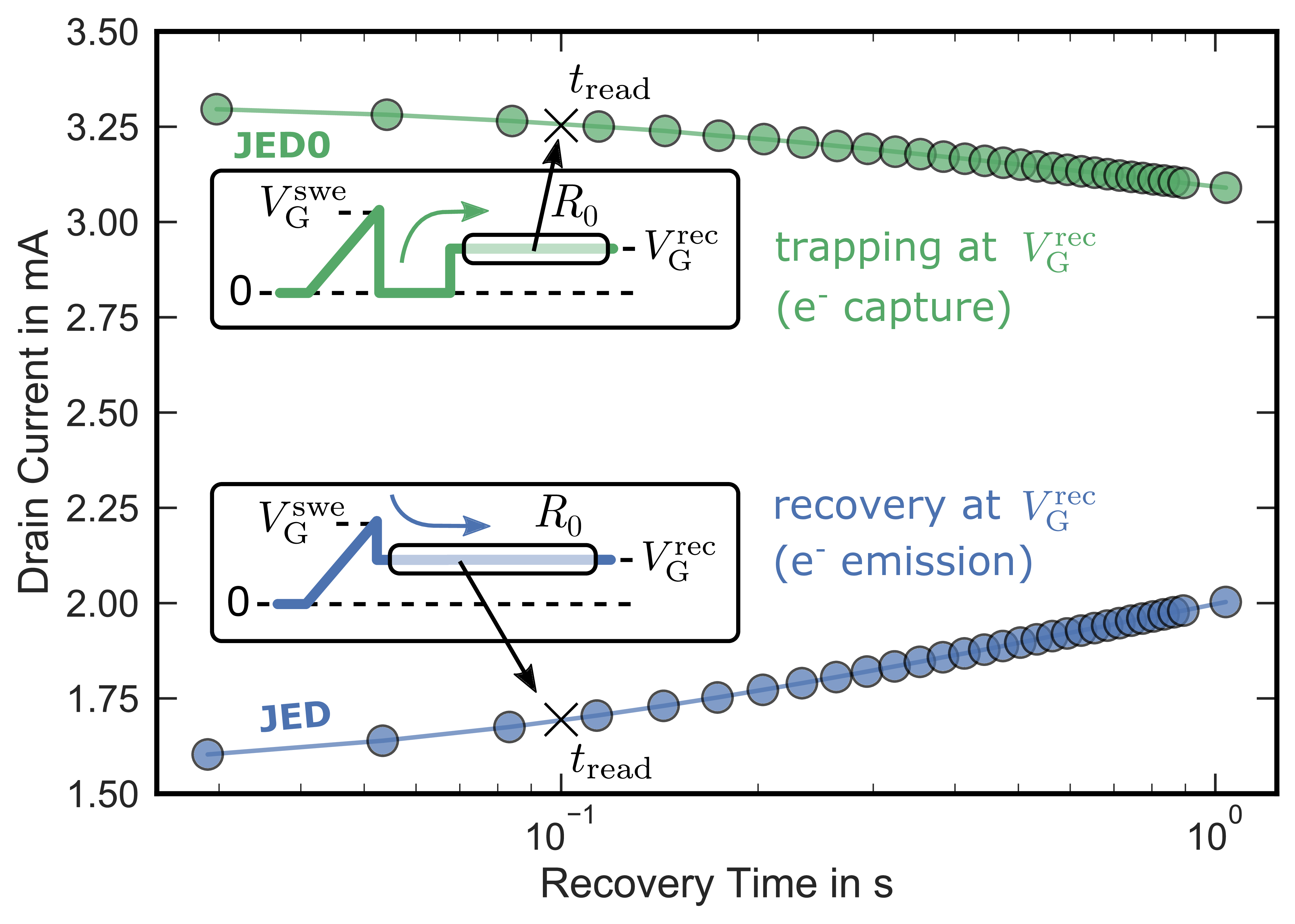
Figure 3.10: Drain current at the reference readout for JED (blue, bottom) and JED0 (green, top).
Trapping or detrapping behavior depends on the preceding gate bias. After the 0 V phase, is higher and decreases over time (JED0, electron
capture), whereas after the switch from to , the drain current is lower and increases over time
(JED, electron emission).
3.3.2 The impact of measurement delay times on
In addition to a well defined reference readout , the timing of each subsequent extraction point after the stress cycle is of similar importance.
An example for a delayed , JEDEC-like readout is given in Fig. 3.11 (referred to as JEDd). The measurement pattern is similar to the JED pattern in Fig. 3.7, extended with a delay phase at for the delay time  after the stress cycle. Especially in industrial reliability tests, delayed measurements
are very common since the stress cycle is usually done in special high temperature furnaces (accelerated BTI stress [130]) where many chips can be stressed in parallel for long times (e.g. 1000 h), whereas the readout is done
outside the furnace sequentially for multiple devices at room temperature. The whole procedure of loading and unloading packaged devices naturally introduces a delay time between the termination of the stress and the extraction point .
after the stress cycle. Especially in industrial reliability tests, delayed measurements
are very common since the stress cycle is usually done in special high temperature furnaces (accelerated BTI stress [130]) where many chips can be stressed in parallel for long times (e.g. 1000 h), whereas the readout is done
outside the furnace sequentially for multiple devices at room temperature. The whole procedure of loading and unloading packaged devices naturally introduces a delay time between the termination of the stress and the extraction point .
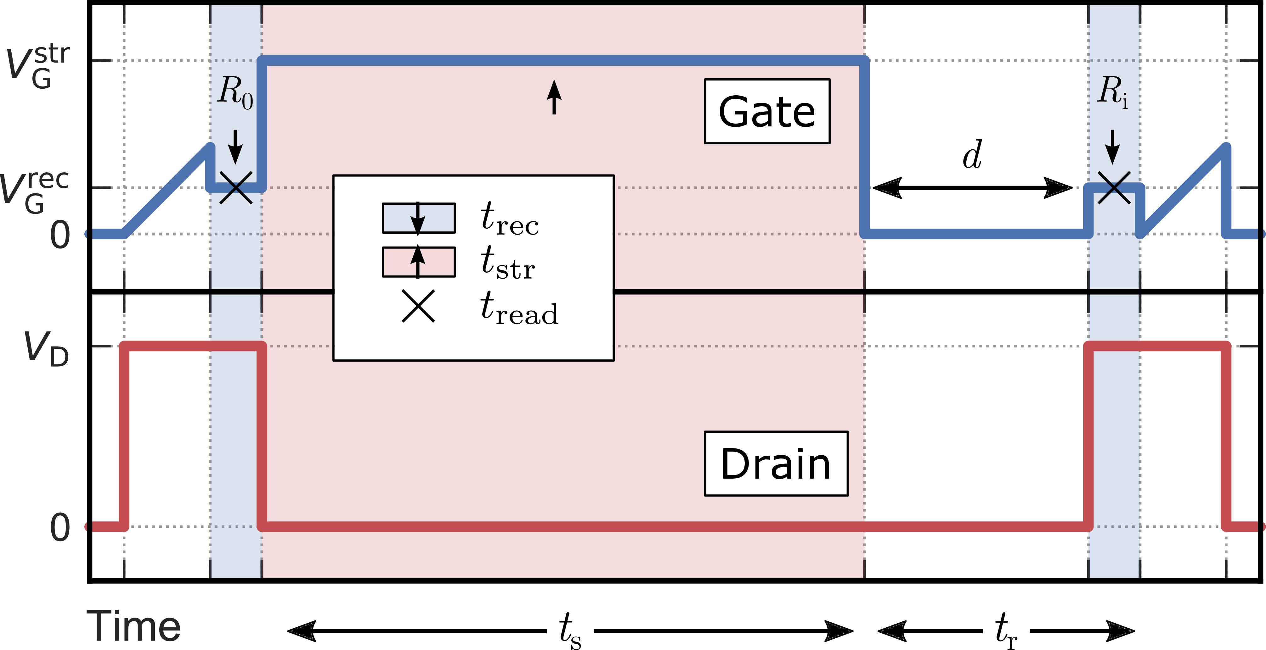
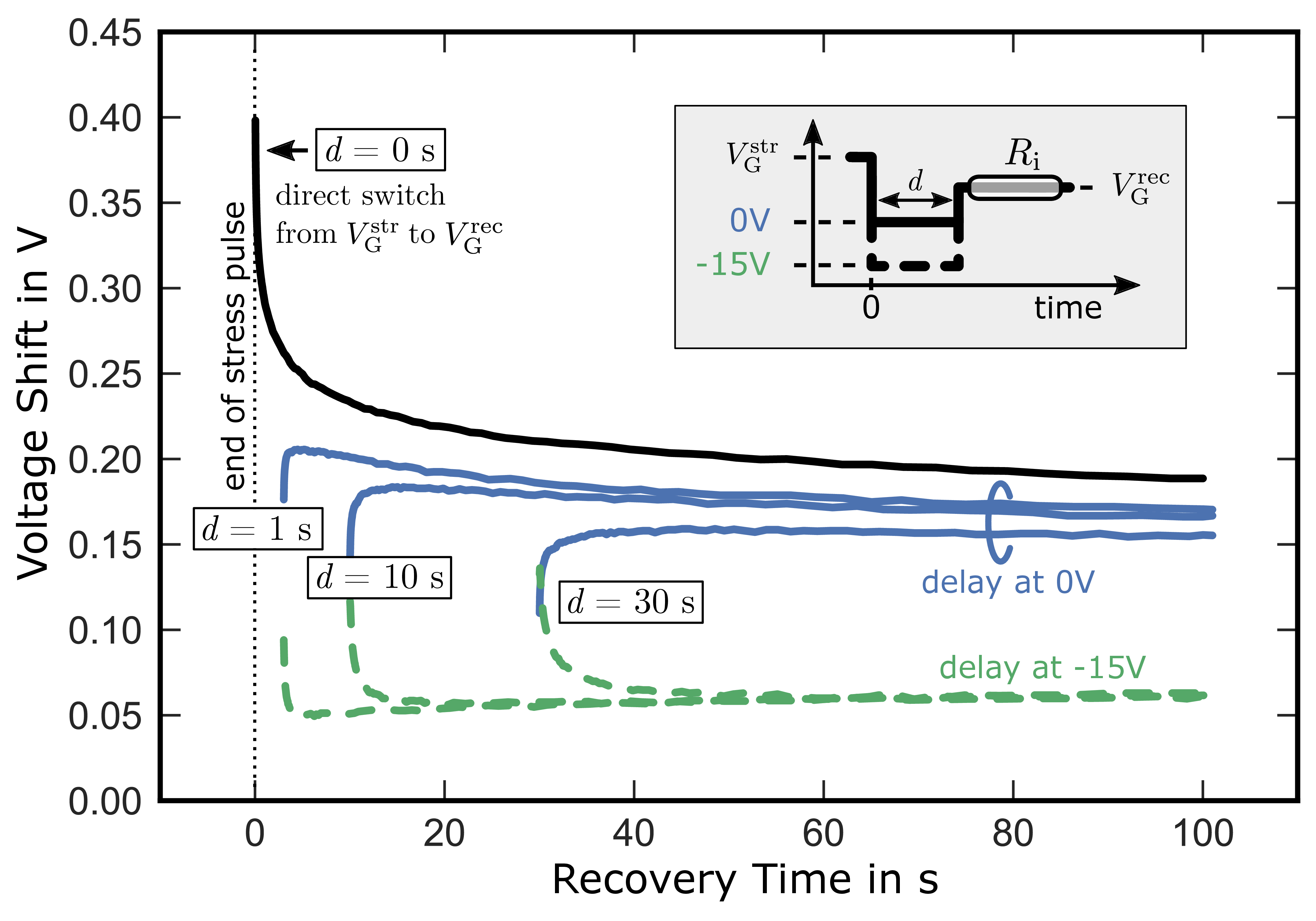
Figure 3.12: Recovery behavior after identical positive bias stress depending on the delay time . The black solid line represents with  (direct switch from to ). By introducing a delay phase at between the stress and the re-
covery phase, decreases with increasing delay time (blue). The measurement procedure is indi-
cated in the inset.
(direct switch from to ). By introducing a delay phase at between the stress and the re-
covery phase, decreases with increasing delay time (blue). The measurement procedure is indi-
cated in the inset.
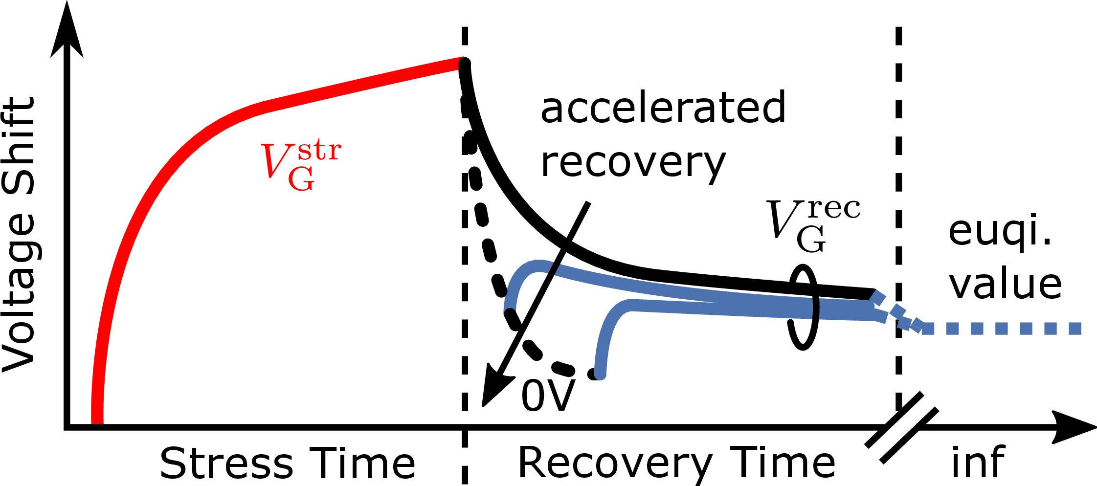
Figure 3.13: Schematic recovery behavior after identical positive bias stress depending on the delay time . The increased recovery mechanism is explained via a steeper recovery curve at (dashed, black). This effect is
increased by using an accumulation pulse during , which results in less dependence of on as indicated in Fig. 3.12.
The impact of on is shown in Fig. 3.12 for multiple devices subjected to identical BTI stress. is measured according to Fig. 3.11 (JEDd). The delay time varies from 0 s to 30 s (black, blue). We see a decreasing voltage shift
for increasing delay times. An explanation is given schematically in Fig. 3.13: the change in is caused by varying Fermi level positions prior to the extraction. As such, increases with stress time according to (1.4) (red) during the stress cycle at . By directly switching to the recovery gate bias
without any delay ( ), follows the black recovery curve according to (1.6). By introducing a delay at , moves from a position close to the conduction
band
), follows the black recovery curve according to (1.6). By introducing a delay at , moves from a position close to the conduction
band  to a position around the
midgap
to a position around the
midgap  leading to emission of trapped
charges with energetic positions above , which results in a decrease of
(dashed black). A subsequent bias change back to (blue) will lead to a superposition of charge
trapping for trap states with energetic positions below
leading to emission of trapped
charges with energetic positions above , which results in a decrease of
(dashed black). A subsequent bias change back to (blue) will lead to a superposition of charge
trapping for trap states with energetic positions below  and above (visible as the rising edge)
and the ongoing charge transition of states above which have not yet emitted
their charge within . As can be seen, the delayed recovery curve approaches a value smaller than recorded
in the non-delayed trace (cf. Fig. 3.12). This effect depends strongly on the delay time and shows that the delay phase at 0 V increases
recovery in comparison to . The same trend is observed for a floating gate
contact during (not shown), as would be the case in typical industrial measurements.
and above (visible as the rising edge)
and the ongoing charge transition of states above which have not yet emitted
their charge within . As can be seen, the delayed recovery curve approaches a value smaller than recorded
in the non-delayed trace (cf. Fig. 3.12). This effect depends strongly on the delay time and shows that the delay phase at 0 V increases
recovery in comparison to . The same trend is observed for a floating gate
contact during (not shown), as would be the case in typical industrial measurements.
A feature that will be exploited in the following is the fact that is further decreased by using an accumulation pulse instead of
0 V/floating (Fig. 3.12, dashed, green) during the delay phase. In this example an accumulation pulse of −15 V is used for the
same range of delay times resulting in a decrease of from  to approximately
  after
after  .
.
3.3.3 Preconditioned BTI
As mentioned before, BTI measurements of SiC-MOSFETs are highly sensible to the exact bias and timing conditions of each voltage shift readout (Fig. 3.12). Therefore, no reliable estimation of a permanent component of can be given. This is due to two essential facts: first, the extracted voltage shift
depends on the reference readout timing and gate bias history since thermal
equilibrium is not reached within a reasonable period of time, meaning a drain current transient is still noticeable due to ongoing charge capture/emission during . Second, the switching condition of each
additional readout usually differs from the switching condition of
. For example in the JEDEC JESD 241 standard
(Fig. 3.7), is monitored after the end-of-sweep voltage , whereas following readouts are monitored after the stress voltage . Therefore, the interface charging state differs
for each readout, resulting in a stress independent offset in the extracted .
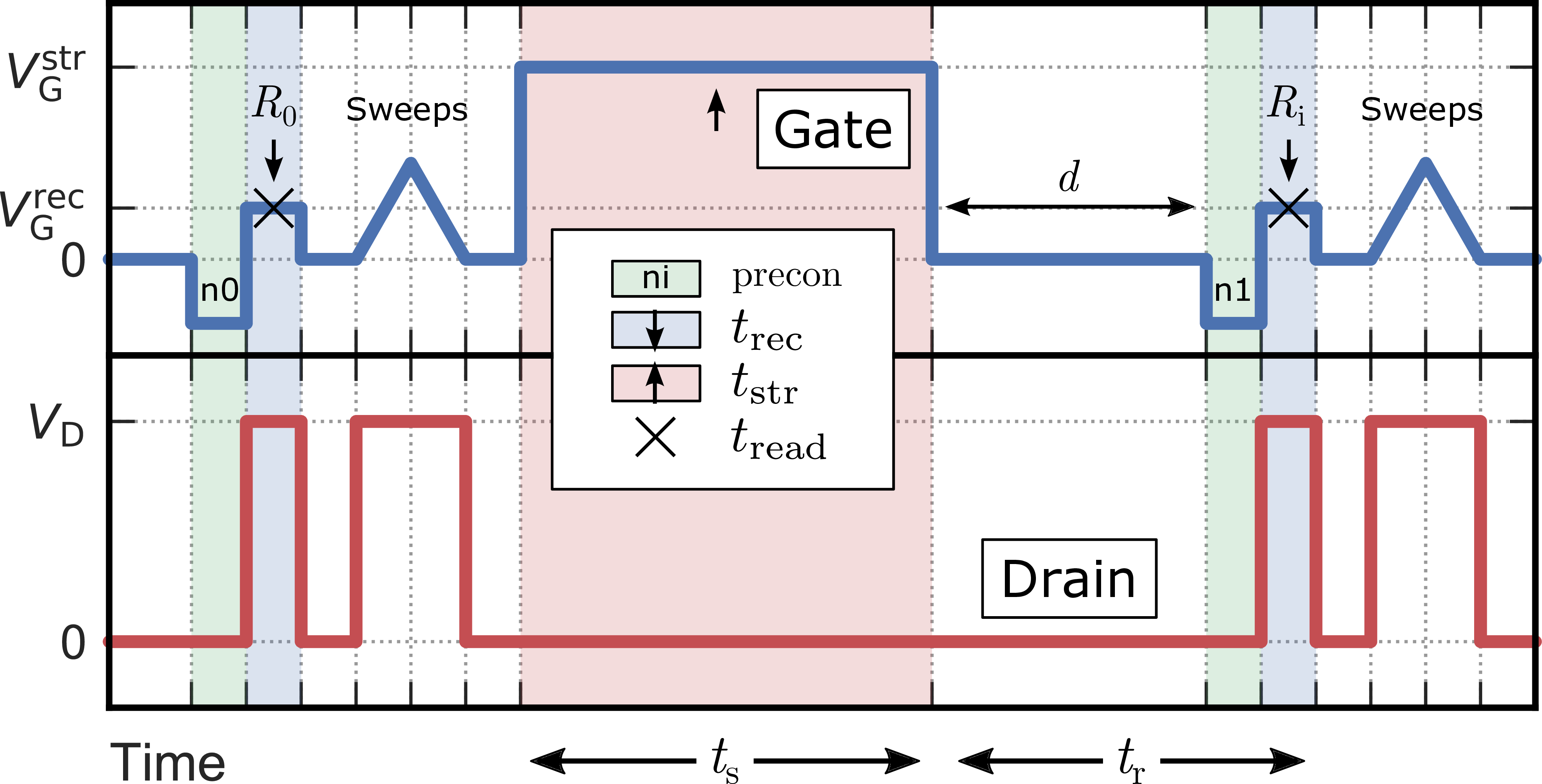
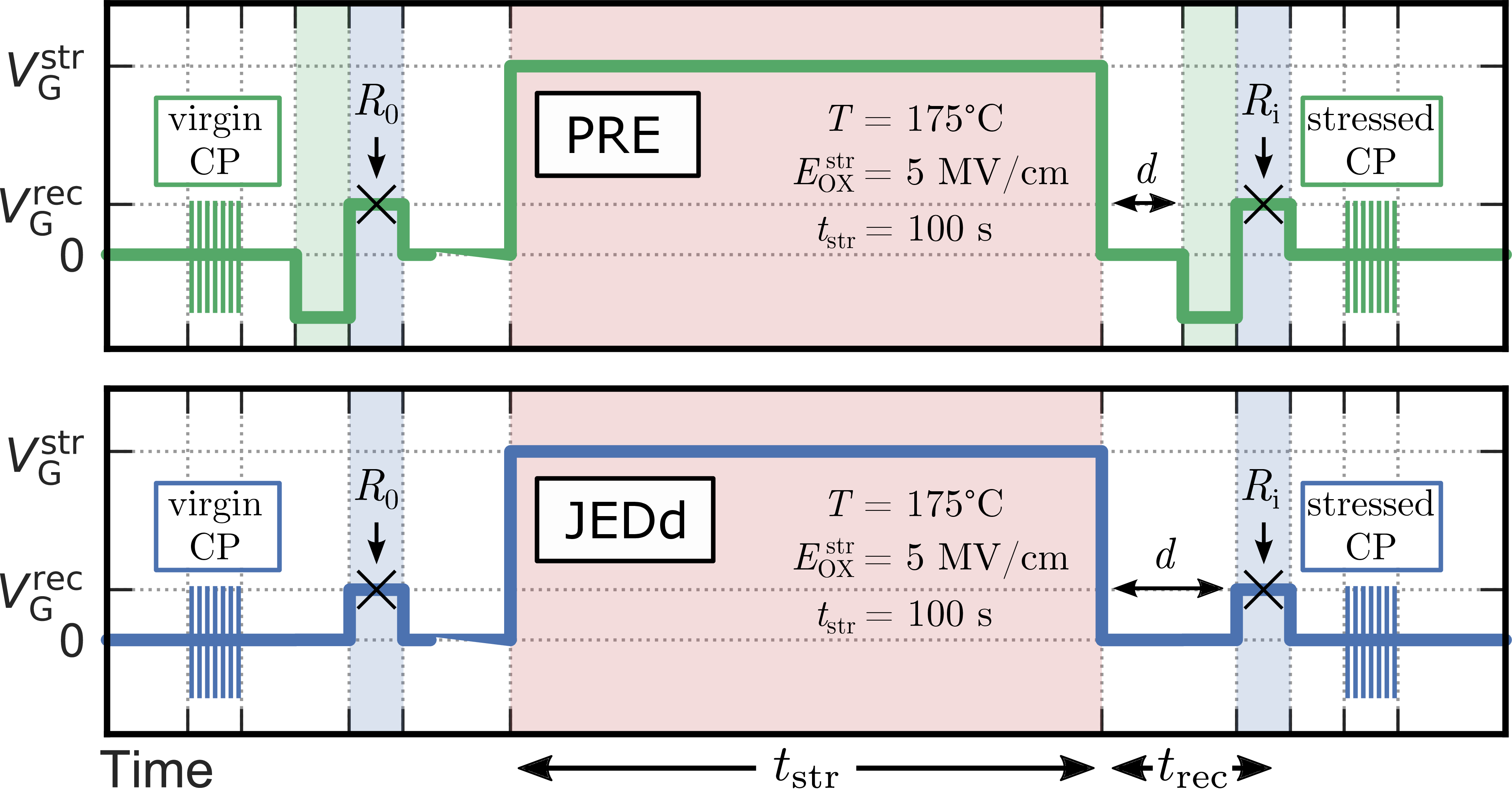
To overcome timing and bias dependent variations of , an optimized measurement pattern is proposed which is refer to as device
preconditioning. The basic scheme is sketched in Fig. 3.14 for a positive bias stress pattern and consists of the following features: first, exactly the same
accumulation preconditioning pulse before each readout cycle is introduced to ensure a well defined and comparable interface charge state at the instant is switched to . By this, one isolates fast interface states
(charging state is able to follow the gate signal) from application-relevant border states with slower time constants allowing for an extraction of nearly independent of the delay time as will be shown in the next section. Second, voltage sweeps (if needed for the
calculation of ), are moved after the readout. Therefore, the bias sweep does not influence the
charge state of the trapping centers during the readouts, allowing for a more comparable voltage shift extraction.

3.3.4 Consequences of preconditioning
For further investigation of the impact of the suggested preconditioning measurement PRE (see Fig. 3.14) on the extraction, we compare the outcome of various "reference readout" and "readout after stress" variations on the voltage shift recovery curves.
The complete measurement pattern with the various investigated readout patterns, and , are shown in Fig. 3.15. Here, we start with an ID -VG sweep (SWE) for the calculation of to include its impact on the subsequent readouts. For the reference readout
we either use a bias switch from to (JED0, purple) or a preconditioned
accumulation pulse readout as shown in Fig. 3.14 with a bias switch from  to
to  (for the preconditioning time
  ) to
) to  , which we refer to as n0 (green). After the
reference-readout, the device is subjected to a positive bias stress of 5 MV/cm for a stress time of
, which we refer to as n0 (green). After the
reference-readout, the device is subjected to a positive bias stress of 5 MV/cm for a stress time of  (STR). After the
stress pulse STR, extraction is done according to JEDEC JESD 241 by switching from to (JED1, blue) or via accumulation pulse
preconditioning identical to n0, referred to as n1 (green).
(STR). After the
stress pulse STR, extraction is done according to JEDEC JESD 241 by switching from to (JED1, blue) or via accumulation pulse
preconditioning identical to n0, referred to as n1 (green).
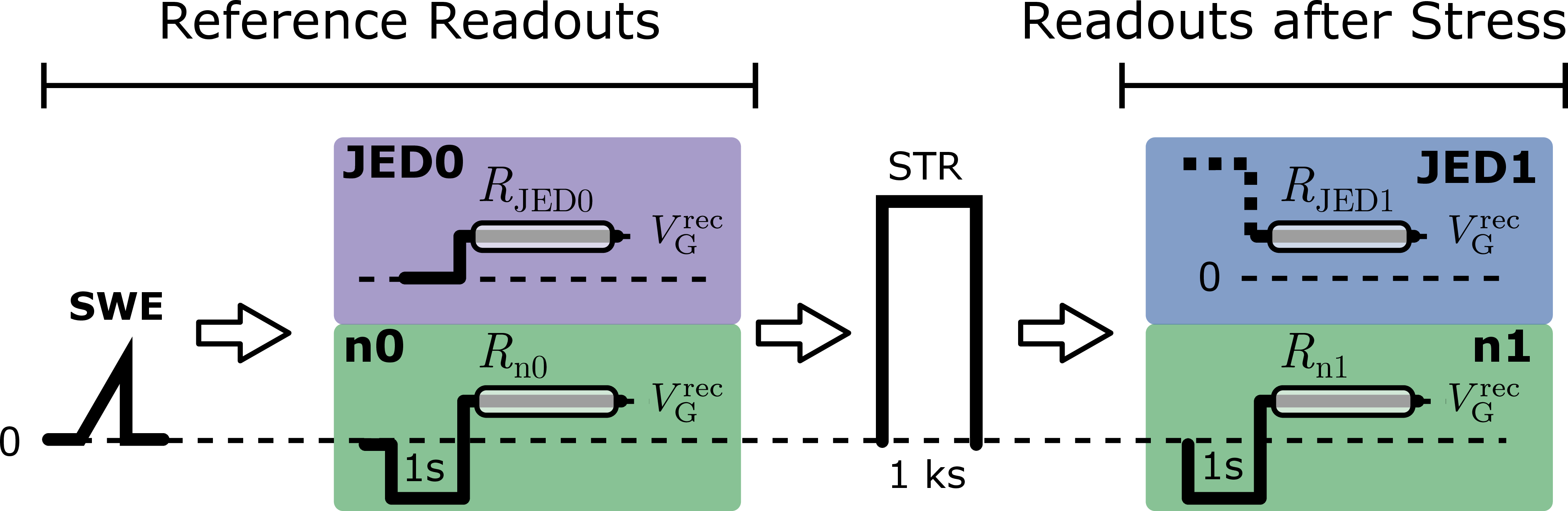
Figure 3.15: Readout variations for the extraction of the voltage shift. For the reference readouts, we either use the sweep (SWE), a JEDEC-like readout with a bias switch from to (JED0, purple) or the preconditioning method
with a preconditioning time of 1 s at −15 V (n0, green). After the stress, is extracted via a direct bias switch from the stress voltage to the readout voltage
(JED1, blue) or via accumulation pulse preconditioning similar to n0 (n1, green).
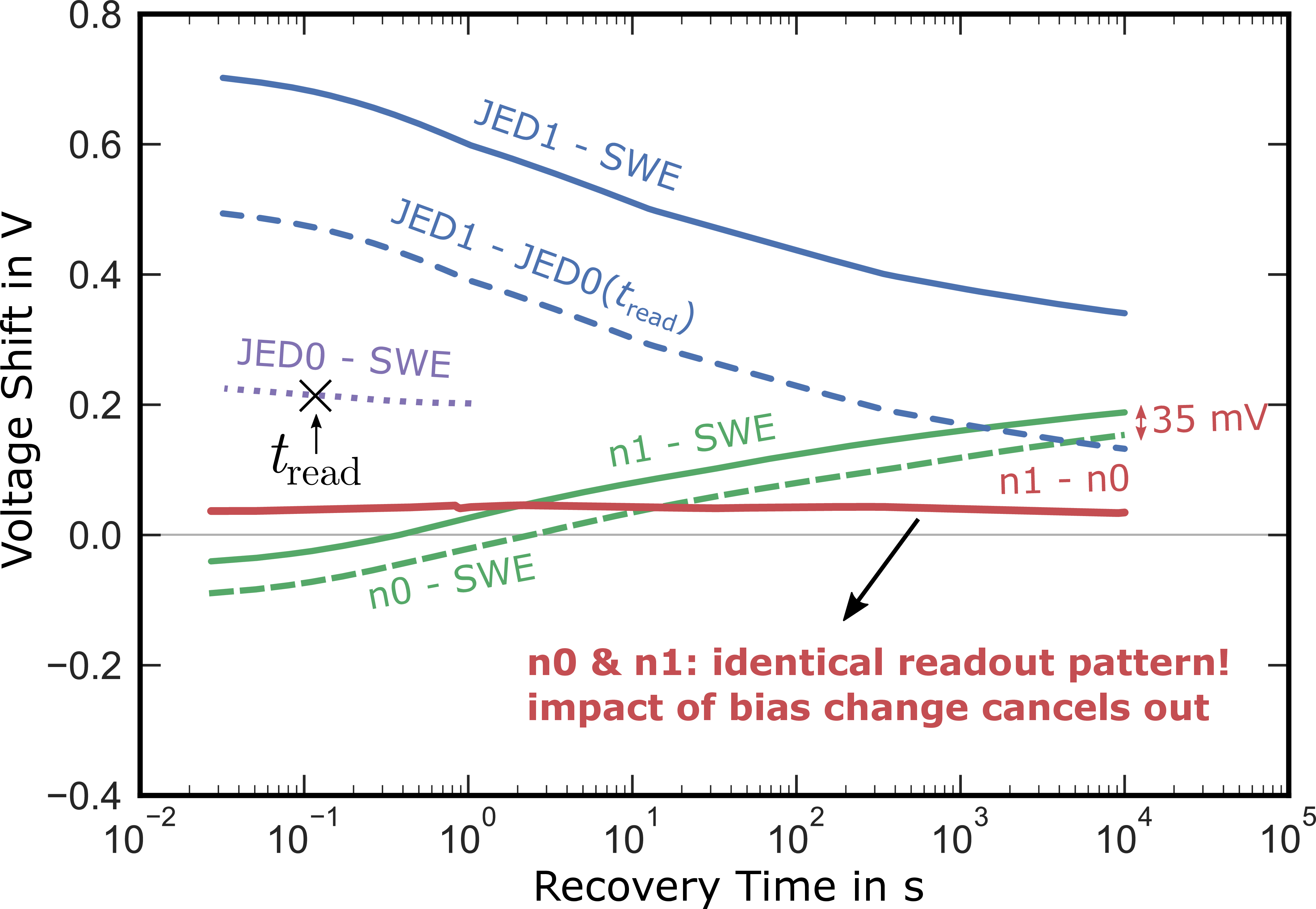
Figure 3.16: Resulting as a function of the chosen extraction pattern according to Fig. 3.15.
strongly depends on the recovery time and stress independent switching conditions
in measurements without preconditioning (blue). On the other hand, using preconditioned measurements results in less recovery time dependence and a more exact extraction due to identical and therefore comparable switching conditions before
each readout (green and red).
The corresponding voltage shift recovery traces are given in Fig. 3.16. Each recovery curve is given relative to one of the reference readouts
JED0, n0 or SWE (indicated by the minus sign). At first, we start by analyzing the reference readout JED0, a simple bias change from 0 V to . As already discussed before and shown in Fig.
3.10, the drain current at  changes over time and can be
converted to a voltage shift by using the sweep SWE as reference. The outcome is shown in Fig. 3.16 as dotted purple line (JED0-SWE). In the JESD 241 measurement standard and numerous other studies, only a certain point in time
changes over time and can be
converted to a voltage shift by using the sweep SWE as reference. The outcome is shown in Fig. 3.16 as dotted purple line (JED0-SWE). In the JESD 241 measurement standard and numerous other studies, only a certain point in time  is used as the reference point for the calculation
of after bias stress. Due to this major drawback of JEDEC-like measurements,
changes drastically in amplitude and time dependence if is changed. In our case, represents the interface charge state
100 ms after switching to .
is used as the reference point for the calculation
of after bias stress. Due to this major drawback of JEDEC-like measurements,
changes drastically in amplitude and time dependence if is changed. In our case, represents the interface charge state
100 ms after switching to .
By using either SWE or JED0() as reference point, we are now able to extract
induced by the stress phase STR as a function of the recovery time  . Fig. 3.16 shows the change with respect to SWE (solid, blue) or JED0() (dashed, blue). Both curves only differ by an
offset of
. Fig. 3.16 shows the change with respect to SWE (solid, blue) or JED0() (dashed, blue). Both curves only differ by an
offset of  , which
originates from the voltage shift of JED0 at . The same effect was already shown in Fig. 3.8.
, which
originates from the voltage shift of JED0 at . The same effect was already shown in Fig. 3.8.
Compared to JED1 recovery curves of the voltage shift (blue), the recovery time dependence of changes drastically if we switch to the accumulation pulse preconditioned readout
and, more importantly, always compare within identical time frames, meaning equals . The solid and dashed green curves represent
at the readouts n0 and n1 with respect to SWE. The difference between n0 and
SWE (n0-SWE) shows before the stress, whereas the difference between n1 and SWE (n1-SWE) shows
after the stress. Since both readouts are performed under identical and well
defined switching conditions from accumulation to inversion, n0 and n1 show the same trend over time. This indicates that the form of the recovery curve mainly depends on the switching conditions since STR does not result in any
noticeable change in the time dependence of the recovery. The difference between both curves represents the real BTI due to the
stress pulse, since any impacts from stress independent switching conditions cancel out. The resulting is indicated in red and is nearly stable at 35 mV within the measured
recovery time of 10 ks, giving a good estimation for the permanent component . The comparison with the JEDEC-like
measurement (given by the difference between JED1 and JED0), which shows a of  recovering to 140 mV within the same
recovery time, proves the importance of comparing pairs of values (,
recovering to 140 mV within the same
recovery time, proves the importance of comparing pairs of values (,  ) rather than prior and after the stress for reliable voltage shift measurements. In particular for
industrial measurements, it is usually sufficient to extract only one pair of values instead of the complete recovery transient as long as
) rather than prior and after the stress for reliable voltage shift measurements. In particular for
industrial measurements, it is usually sufficient to extract only one pair of values instead of the complete recovery transient as long as  .
.
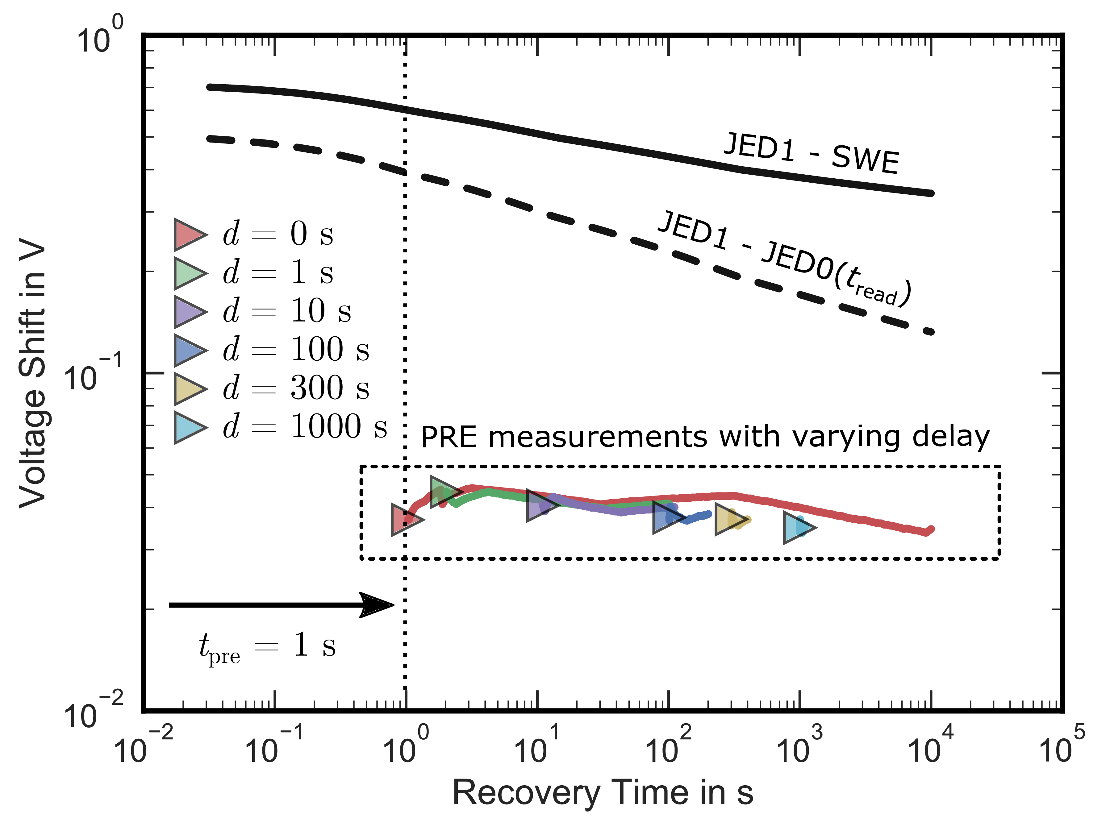
Figure 3.17: Same as Fig. 3.16 but with delay times ranging from  (red) to
  (cyan) at 0 V. extracted via preconditioned measurements shows only a minor dependence on the
delay time. Preconditioning was performed for (black arrow).
(cyan) at 0 V. extracted via preconditioned measurements shows only a minor dependence on the
delay time. Preconditioning was performed for (black arrow).
In addition to the accurate determination of , preconditioned measurements are more robust to delay time variations. Fig. 3.17 shows the data from Fig. 3.16 on a logarithmic y-axis
with additional data for delay times between STR and n1 ranging from (red) to (cyan). During the delay time, the gate voltage is fixed to
0 V. depends only slightly on the delay time and stays within 35 mV and
45 mV. A more comprehensive picture on the delay time dependence is given in the next section.
3.3.5 Minimized impact of delay times
Especially in industrial BTI measurements with a large number of devices stressed simultaneously, delay times between the end of the stress pulse and the readout are inevitable. Delay times lead to a large
inaccuracy in the extracted in JEDEC-like measurement due to ongoing recovery, as shown in Fig. 3.12. Preconditioned BTI measurements, on the other hand, show much less dependence of on the delay time between the end of the stress pulse and the beginning of the
readout pulse , allowing for more reliable extraction of
application-relevant voltage shift.

Fig. 3.18 shows the delay time dependence of for a 10 h, 5 MV/cm positive bias stress at 150 °C
for delay times up to 1 h, which is in the range of typical industrial delay times. The delayed JEDEC-like measurement JEDd (see Fig. 3.11) is
shown in blue circles, whereas the preconditioned measurements (according to Fig. 3.14) are shown with triangles labeled PRE. Readout was done at
150 °C (green and blue) or 30 °C with cooldown under (red) or floating (purple). JEDd exhibits a
strong dependence of on and recovers from 560 mV for  to 320 mV for
  , representing a recovery slope of
  at a recovery
temperature of 150 °C. The preconditioned measurement at the same recovery temperature is shown in green triangles and represents after identical stressing conditions. Since recoverable components, which are
irrelevant for application, are eliminated, shows a 5 times smaller dependence on the delay time and ranges from
190 mV for
at a recovery
temperature of 150 °C. The preconditioned measurement at the same recovery temperature is shown in green triangles and represents after identical stressing conditions. Since recoverable components, which are
irrelevant for application, are eliminated, shows a 5 times smaller dependence on the delay time and ranges from
190 mV for  to 155 mV for with slopes smaller than
  . The red curve
represents PRE with readout performed at 30 °C and cooling down under resulting in higher shift and less recovery but
identical dependence on the delay time. The purple data represents after cooling down performed under floating conditions, which results in data
points shifted to longer delay times since the time needed to reach 30 °C adds to the delay time.
. The red curve
represents PRE with readout performed at 30 °C and cooling down under resulting in higher shift and less recovery but
identical dependence on the delay time. The purple data represents after cooling down performed under floating conditions, which results in data
points shifted to longer delay times since the time needed to reach 30 °C adds to the delay time.
3.3.6 The impact of the preconditioning time
The impact of the preconditioning time  was investigated using the measurement pattern
sketched in Fig. 3.19. Here, we compare after a 100 s positive bias stress and 5 MV/cm for a
measurement without preconditioning (top), and measurements with varying preconditioning times (bottom). For the measurement without
preconditioning the recovery of the voltage shift was recorded up to 100 s, allowing for a comparison to measurements with preconditioning times up to
was investigated using the measurement pattern
sketched in Fig. 3.19. Here, we compare after a 100 s positive bias stress and 5 MV/cm for a
measurement without preconditioning (top), and measurements with varying preconditioning times (bottom). For the measurement without
preconditioning the recovery of the voltage shift was recorded up to 100 s, allowing for a comparison to measurements with preconditioning times up to  . After the
preconditioning pulse, was recorded for 10 s. For all measurements in this section, the delay
time was set to at . Preconditioning was
performed via an accumulation pulse at
. After the
preconditioning pulse, was recorded for 10 s. For all measurements in this section, the delay
time was set to at . Preconditioning was
performed via an accumulation pulse at  for preconditioning times
ranging from 0.1 s to 100 s. Temperature was fixed to 175 °C during the entire process.
for preconditioning times
ranging from 0.1 s to 100 s. Temperature was fixed to 175 °C during the entire process.
Figure 3.19: Schematics for the measurement of the impact of the negative preconditioning time on the resulting voltage shift. The measurement
pattern without preconditioning is given in the top, whereas the pattern with varying preconditioning time is indicated at the bottom. The delay time for both measurement patterns was set to 1 s.
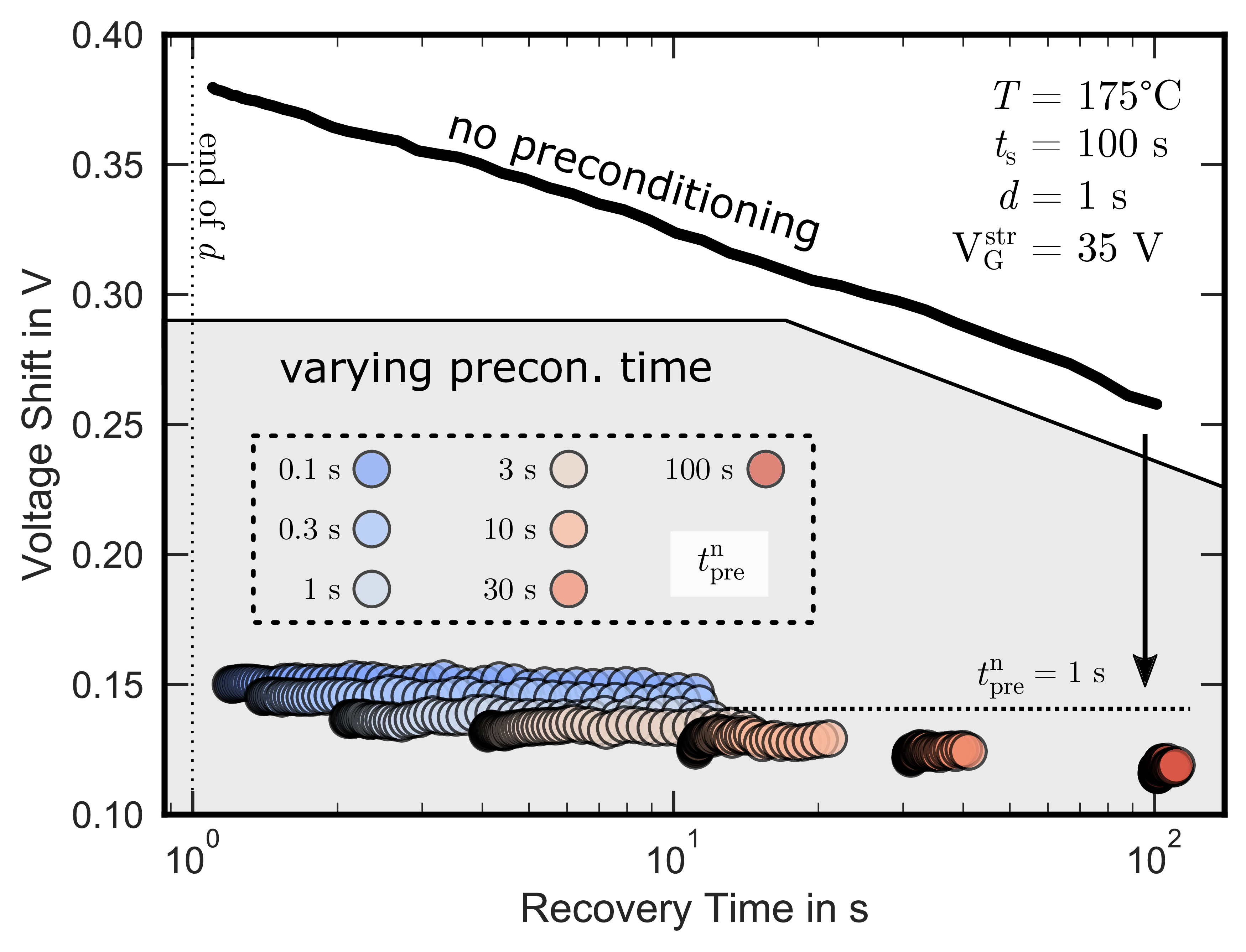
Figure 3.20: Impact of the preconditioning time varying from 0.1 s (circles, blue) to 100 s
(circles, red) on at 175 °C. The preconditioning was always performed in accumula-
tion at . The solid black line repre-
sents the recovery curve for a measurement without preconditioning. As for the stress and
recovery time, scales with the logarithm of . Therefore, even a short decreases the recovery time by several orders of
magnitude. Delay time for all measurements was 1 s.
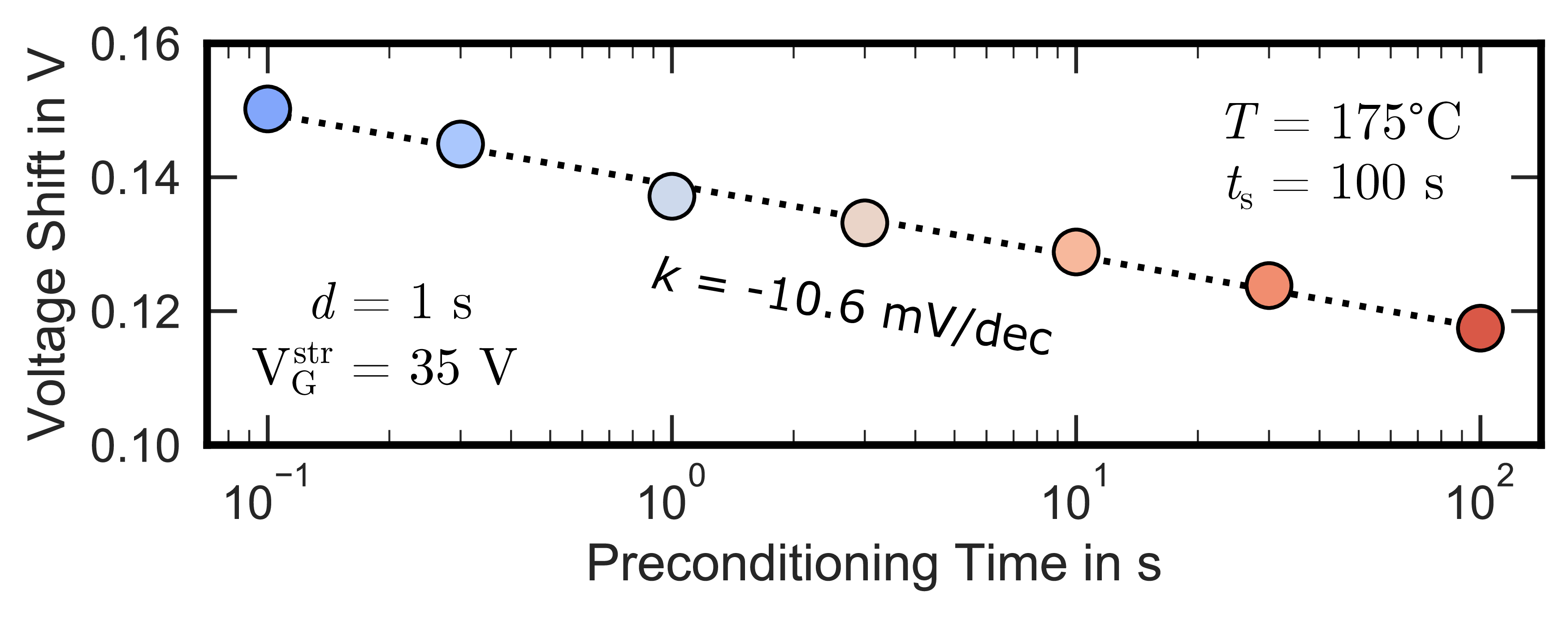
Figure 3.21: Mean value of as a function of extracted from the data in Fig. 3.20
for ranging from 0.1 s (blue) to 100 s
(red). Increasing by one order of magnitude reduces by approximately 10.6 mV.
Fig. 3.20 shows the impact of on the voltage shift. Here, the solid line
represents without a negative preconditioning pulse. Within two orders of magnitude in
recovery time, decreases from approximately 380 mV (at  ) to 250 mV (at
 ). For the preconditioned
measurement on the other hand, even a short decreases the recovery time compared to the non-preconditioned measurement by several orders
of magnitude. For example, the 0.1 s preconditioning pulse (circles, blue) is already sufficient to decrease to 150 mV (at ), which is 60 %
lower than the voltage shift in the measurement without preconditioning after 100 s. Furthermore, remains nearly constant during the recovery phase, as already discussed in the
previous section (c.f. Fig. 3.16, red).
). For the preconditioned
measurement on the other hand, even a short decreases the recovery time compared to the non-preconditioned measurement by several orders
of magnitude. For example, the 0.1 s preconditioning pulse (circles, blue) is already sufficient to decrease to 150 mV (at ), which is 60 %
lower than the voltage shift in the measurement without preconditioning after 100 s. Furthermore, remains nearly constant during the recovery phase, as already discussed in the
previous section (c.f. Fig. 3.16, red).
Fig. 3.21 shows the mean value of extracted from the data in Fig. 3.20 within the first 10 s after the end of the preconditioning pulse for ranging from 0.1 s to 100 s.
As for the stress and recovery time, decreases with the logarithm of the preconditioning time . Increasing by one order of magnitude results in
10.6 mV less voltage shift. This proves that the 1 s preconditioning pulse used in this chapter is already a sufficient preconditioning time to decrease the recovery time by several orders of magnitude.
3.3.7 Interface degradation caused by preconditioning
To confirm the correctness of preconditioned measurements, it is necessary to ensure the interface is not damaged by the additional preconditioning pulse itself. Therefore, charge pumping measurements where performed for both
extraction patterns as shown in Fig. 3.22. The charge pumping current  was extracted at a frequency of 50 kHz
before the first readout (virgin) and after the last readout (stressed) for JEDd and PRE using constant base level CP measurements with a low level of the gate pulse of
was extracted at a frequency of 50 kHz
before the first readout (virgin) and after the last readout (stressed) for JEDd and PRE using constant base level CP measurements with a low level of the gate pulse of  and a high level of
  . The stress field was set to
5 MV/cm for
. The stress field was set to
5 MV/cm for  .
.
The outcome is shown in Fig. 3.23. As can be seen, both extraction patterns show similar charge pumping signals (left). The additional 1 s
accumulation pulse used in PRE does not lead to any additional degradation compared to JEDd. For both readout patterns, increases by approximately 1 % after
the 100 s stress at 175 °C.
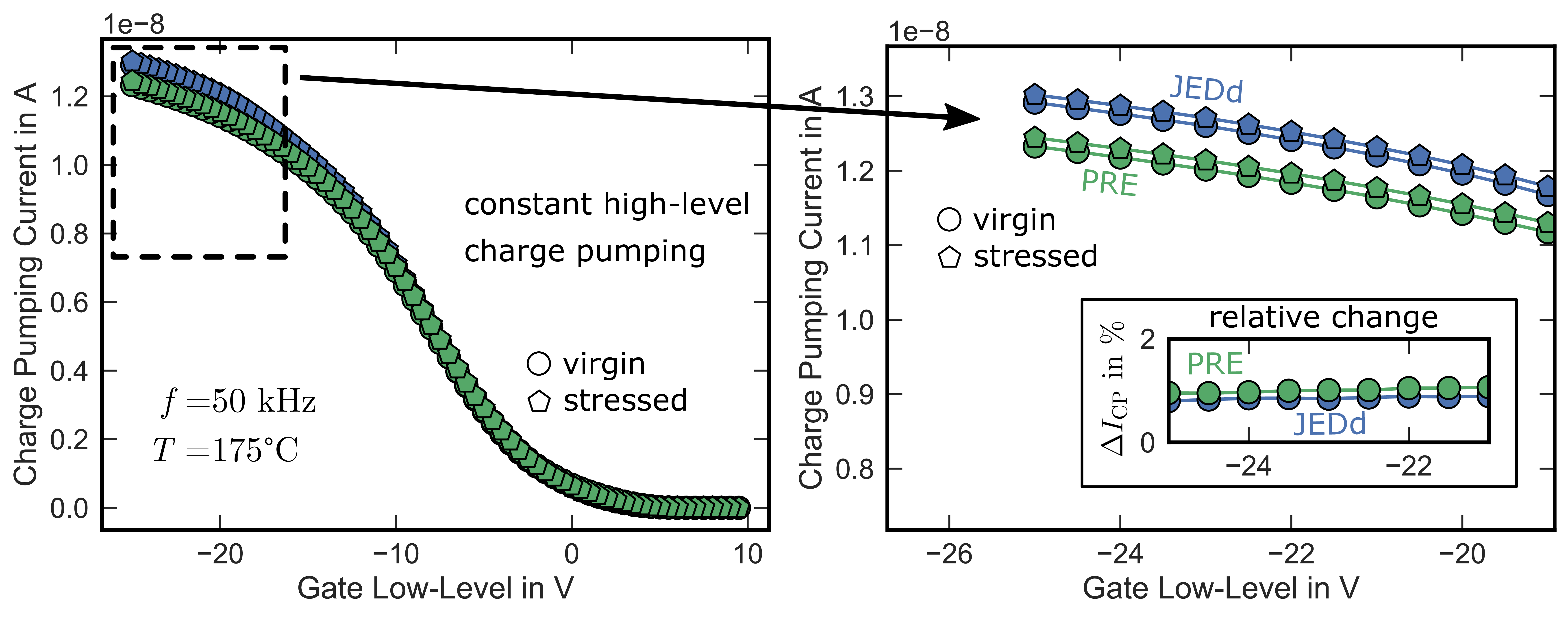
Figure 3.23: Constant high-level charge pumping measurements for JEDd and PRE. The CP measurement was performed according to Fig. 3.22.
increases by approximately 1 % for JEDd
and PRE. The additional accumulation pulse for does not lead to an additional
interface degradation.
3.3.8 Hysteresis monitoring
4H-SiC MOSFETs show a hysteresis (SH) between gate voltage up-sweeps from accumulation to inversion and the down-sweeps from inversion to accumulation, which is especially visible in the sub-threshold regime. The majority
of the hysteresis is caused by charging and discharging of interface states, which is fully recoverable during normal device operation [29, 43, 111]. However, the impact of BTI on the density of interface states  causing the hysteresis has not been investigated
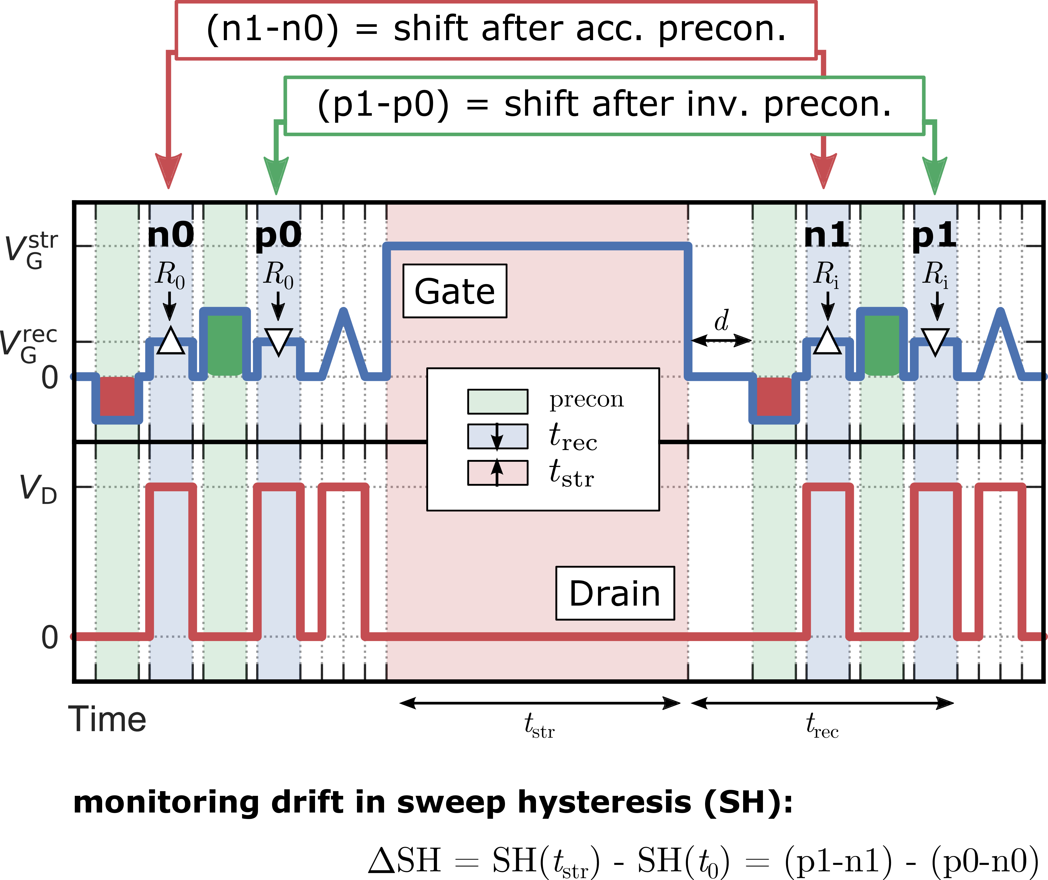
until now. To enable the monitoring of changes in the hysteresis during high temperature gate stress, the accumulation pulse readout n0 is extended via a second inversion preconditioning pulse p0 at use-voltage, resulting in the
measurement pattern shown in Fig. 3.24. By using negative and positive preconditioning pulses, AC-use conditions are mimicked. The hysteresis
before stress is given by the voltage shift after the positive p0 and negative n0 preconditioning, wheres the hysteresis after the stress is given by the difference between p1 and n1. The change in hysteresis due to BTI is therefore given
by
causing the hysteresis has not been investigated
until now. To enable the monitoring of changes in the hysteresis during high temperature gate stress, the accumulation pulse readout n0 is extended via a second inversion preconditioning pulse p0 at use-voltage, resulting in the
measurement pattern shown in Fig. 3.24. By using negative and positive preconditioning pulses, AC-use conditions are mimicked. The hysteresis
before stress is given by the voltage shift after the positive p0 and negative n0 preconditioning, wheres the hysteresis after the stress is given by the difference between p1 and n1. The change in hysteresis due to BTI is therefore given
by  p1
p1 n1
n1 p0n0
p0n0 . Fig. 3.25 shows a comparison of the JEDEC JESD 241 (circles) and the preconditioned BTI after a 1 s accumulation pulse (negative PRE, triangles up)
and after a succeeding 1 s inversion pulse (positive PRE, triangles down) for a 44 h, 5 MV/cm positive stress at 150 °C.
. Fig. 3.25 shows a comparison of the JEDEC JESD 241 (circles) and the preconditioned BTI after a 1 s accumulation pulse (negative PRE, triangles up)
and after a succeeding 1 s inversion pulse (positive PRE, triangles down) for a 44 h, 5 MV/cm positive stress at 150 °C.
For JEDEC readouts, is overestimated for given stress times and depends strongly on because stress independent components are not
excluded. Preconditioned measurements eliminate a large fraction of these components, resulting in an approximately 2.3 times lower and more application-relevant . The difference in for negative and positive PRE results from the hysteresis (red squares), which
slightly increases during high temperature, high field positive bias stress. The fit (dashed) was done according to (1.4)
assuming  [130]. Extracted
parameters of the normally distributed
[130]. Extracted
parameters of the normally distributed  (
( ) are given in the bottom plot. PRE
measurements show significantly reduced standard deviation with
) are given in the bottom plot. PRE
measurements show significantly reduced standard deviation with  .
.
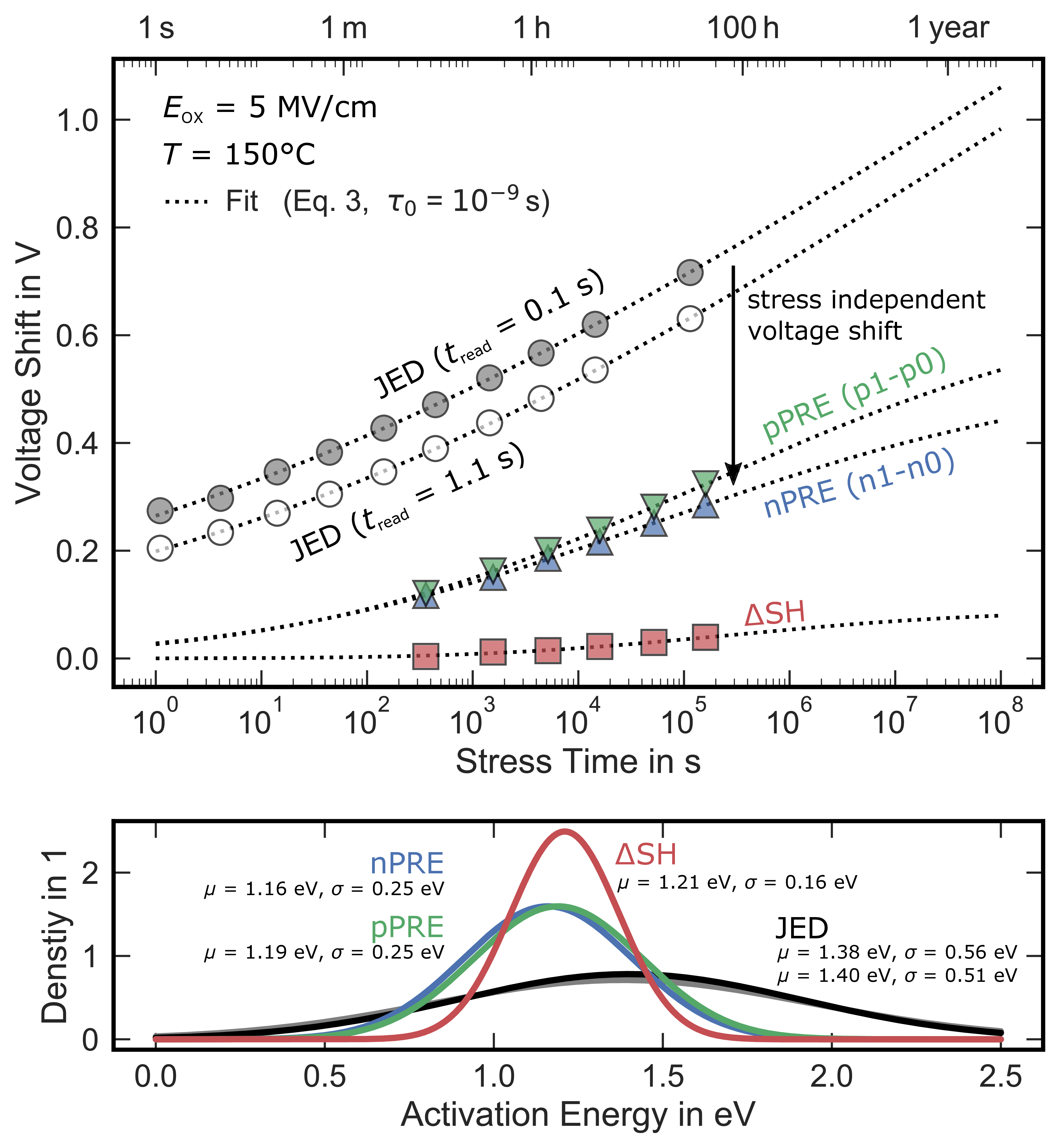
Figure 3.25: Top: voltage shift for stress times up to approximately  for JEDEC JESD 241 (circles) with two different values for and preconditioned BTI according to Fig. 3.24 after negative (nPRE, blue, triangles up) and positive (pPRE, green, triangles down) preconditioning. Although stress conditions are identical,
preconditioned measurements show significantly less shift. The difference between pPRE and nPRE represents the change in sweep hysteresis as a function of the stress time (squares, red). Bottom: parameters of the normally
distributed () are extracted using (1.4) (assuming [130]).
for JEDEC JESD 241 (circles) with two different values for and preconditioned BTI according to Fig. 3.24 after negative (nPRE, blue, triangles up) and positive (pPRE, green, triangles down) preconditioning. Although stress conditions are identical,
preconditioned measurements show significantly less shift. The difference between pPRE and nPRE represents the change in sweep hysteresis as a function of the stress time (squares, red). Bottom: parameters of the normally
distributed () are extracted using (1.4) (assuming [130]).
3.3.9 Conclusions
The impact of various bias temperature instability measurement parameters on the extracted voltage shift of 4H-SiC power MOSFETs was investigated. An accurate BTI procedure should assess exclusive parameter drifts, which
degrade the application-relevant device performance. However, using JEDEC-like measurements, the majority of after high bias stress originates from fully-recoverable and stress independent
shift components, which strongly depend on the measurement parameters and incorrectly add to the extracted . changes drastically by changing the reference point for the shift calculation and
strongly depends on recovery and delay times of the measurement. To overcome this issue, a sophisticated bias temperature instability measurement pattern using device preconditioning is demonstrated, which allows for an exact
determination of the application-relevant voltage shift . By using similar and well defined preconditioning pulses before each readout,
fully-reversible shift components are eliminated, thereby allowing for a more accurate extraction of the application-relevant permanent component. Voltage shifts extracted via preconditioned BTI are still higher but in the range of
silicon based power MOSFETs, less dependent on measurement delay times within industrial timescales, and do not include fully-recoverable hysteresis effects. Therefore, they enable more accurate lifetime prediction of 4H-SiC
MOSFETs.
Previous: 3.2 Similarities in BTI of commercially available SiC-power MOSFETs Top: 3 On the second Component: Bias Temperature Instability Next: 4 Charge accumulation in high temperature processing steps