« PreviousUpNext »Contents
Previous: 2.5 Crystal face dependence Top: 2 On the first Component: the Subthreshold Hysteresis Next: 2.7 Possible atomic origin
2.6 Charge pumping
Because of its high sensitivity to interface states, charge pumping (CP) [82] is a suitable technique to investigate the sweep hysteresis and was recently demonstrated on 4H-SiC MOSFETs in various studies [84–86, 115, 116]. An introduction to the charge pumping measurement techniques as performed in this chapter is given in Section 1.3.4.
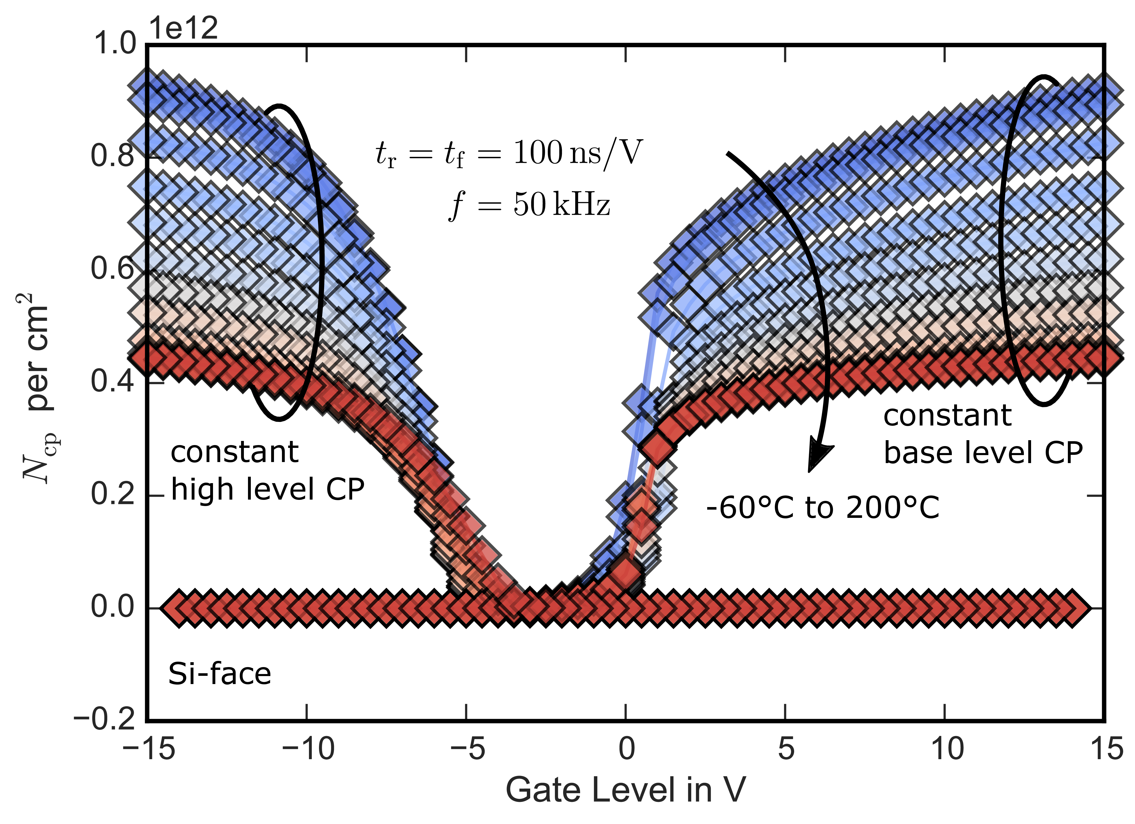
Figure 2.25: Charges pumped per cycle extracted from constant base level CP (right wing) and constant high level CP (left wing) for the Si-face device. The increase in  with decreasing
  originates from trap states close to the band edges of 4H-SiC, which do not con-
tribute to
originates from trap states close to the band edges of 4H-SiC, which do not con-
tribute to  at elevated temperatures due to the narrowing of
the active energy window, as described in Section 1.3.4.
at elevated temperatures due to the narrowing of
the active energy window, as described in Section 1.3.4.
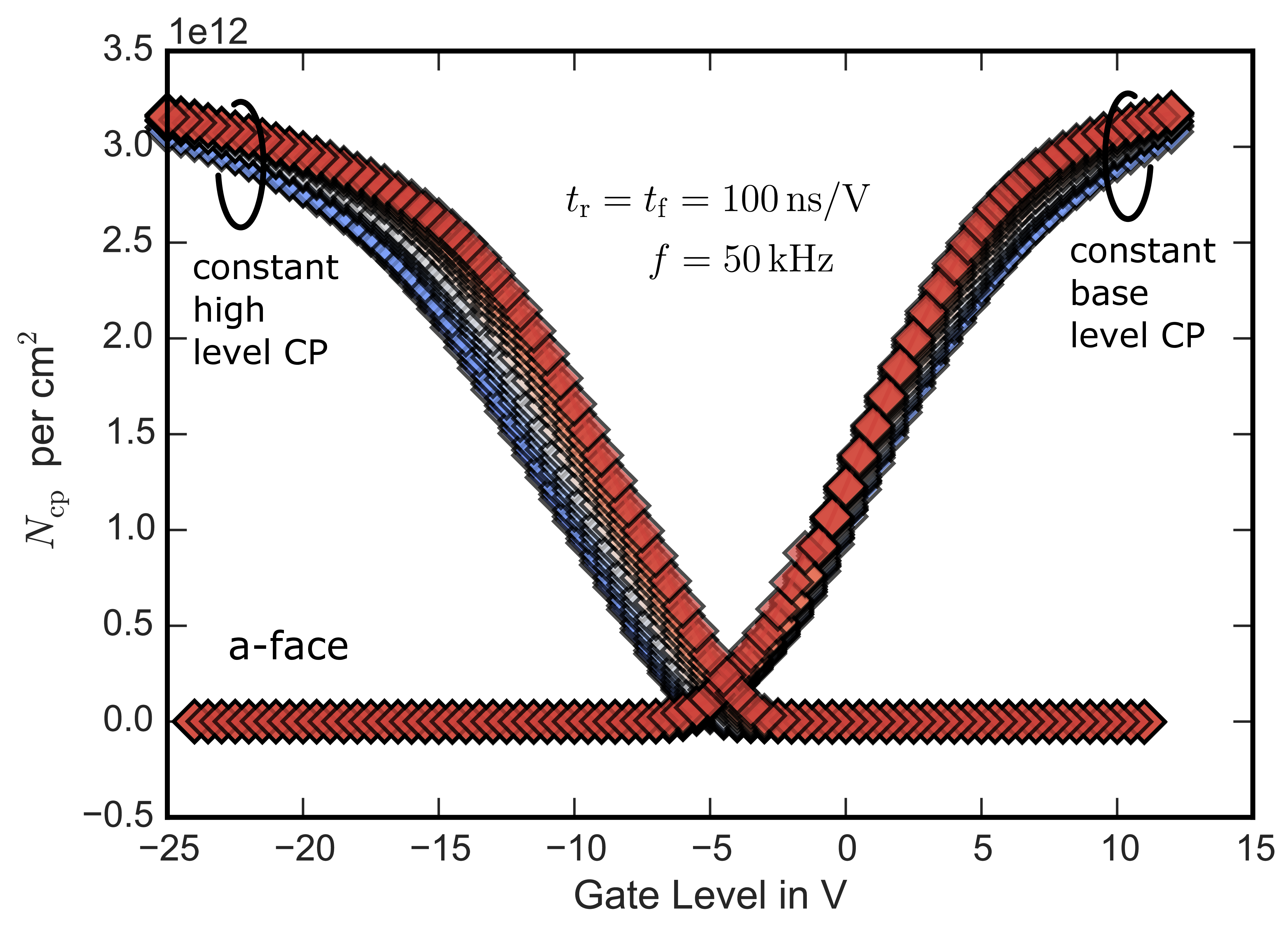
Figure 2.26: Same as Fig. 2.25 but now for the a-face device. We observe a minor dependence of on the temperature and an overall higher signal,
indicating the major contribution to the charge pumping current originates from trap states around midgap.
According to the schematics in Fig. 1.17, constant high level and constant base level CP measurements at a fixed frequency of 50 kHz and fixed transition
rates of  were performed in a wide temperature range between −60 °C and 200 °C. From the charge pumping current , one is able to calculate the number of pumped
charges per cycle via
were performed in a wide temperature range between −60 °C and 200 °C. From the charge pumping current , one is able to calculate the number of pumped
charges per cycle via

with the effective gate area  and the frequency of the gate pulse
  . The outcome, which shows temperature
dependence of the total number of pumped charges per cycle , is presented in Fig. 2.25 for the Si-face device and in Fig. 2.26 for the a-face device. For the former, ranges between
0.4 × 10¹²/cm2 and 0.9 × 10¹²/cm2, strongly depending on the device temperature. If the majority of the CP signal originates from trap states with energetic positions
close to the band edges, this is an expected outcome due to the narrowing of the active energy window
. The outcome, which shows temperature
dependence of the total number of pumped charges per cycle , is presented in Fig. 2.25 for the Si-face device and in Fig. 2.26 for the a-face device. For the former, ranges between
0.4 × 10¹²/cm2 and 0.9 × 10¹²/cm2, strongly depending on the device temperature. If the majority of the CP signal originates from trap states with energetic positions
close to the band edges, this is an expected outcome due to the narrowing of the active energy window  with temperature as described in Section 1.3.4. For the a-face device on the other hand, the total number of pumped charges is approximately 5 times higher (3.0 × 10¹²/cm2) and nearly no temperature
dependence is observed. This indicates the major contribution to the signal originates from trap states which are energetically located around the intrinsic Fermi level (mid-gap) of 4H-SiC.
with temperature as described in Section 1.3.4. For the a-face device on the other hand, the total number of pumped charges is approximately 5 times higher (3.0 × 10¹²/cm2) and nearly no temperature
dependence is observed. This indicates the major contribution to the signal originates from trap states which are energetically located around the intrinsic Fermi level (mid-gap) of 4H-SiC.
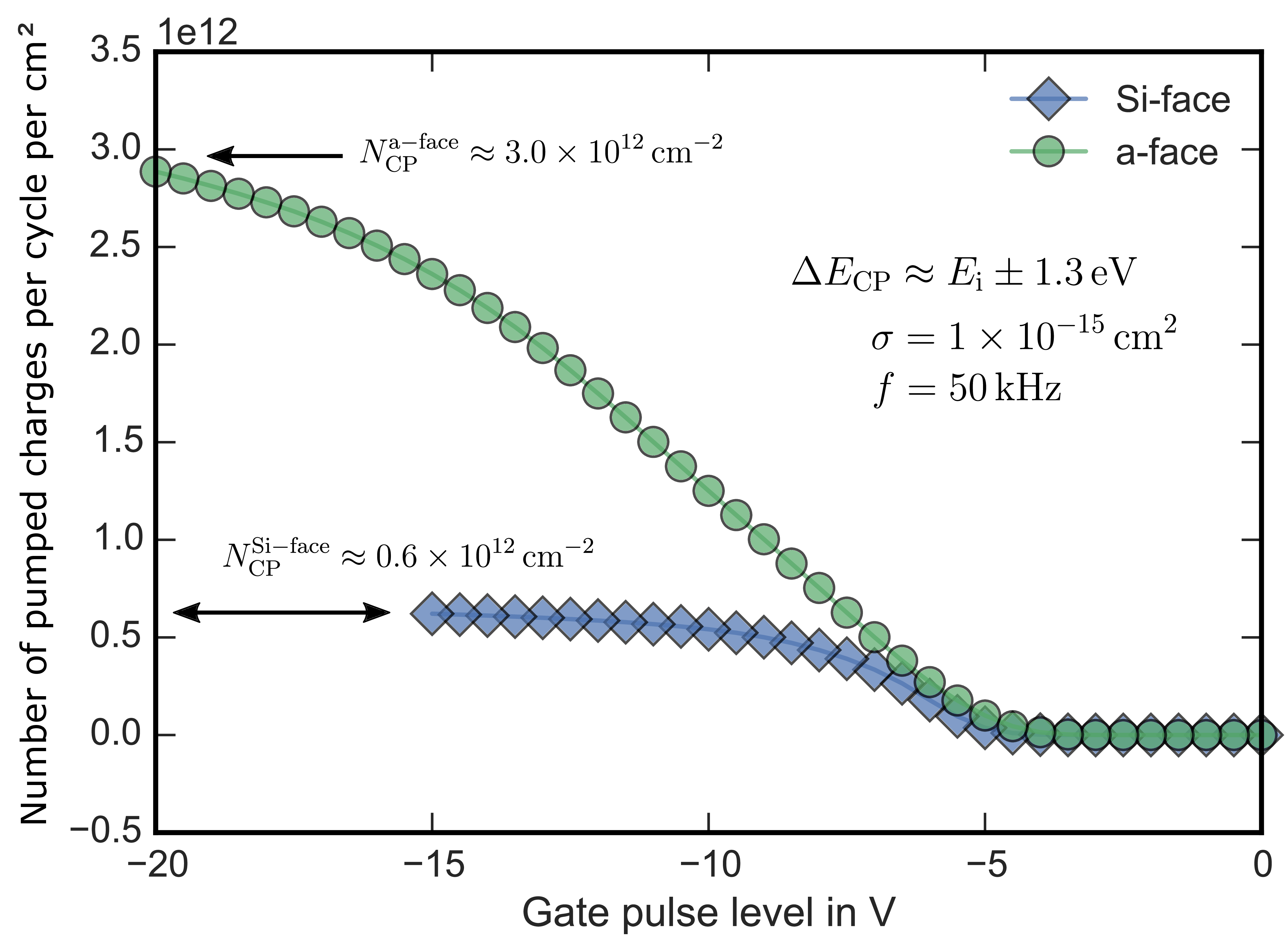
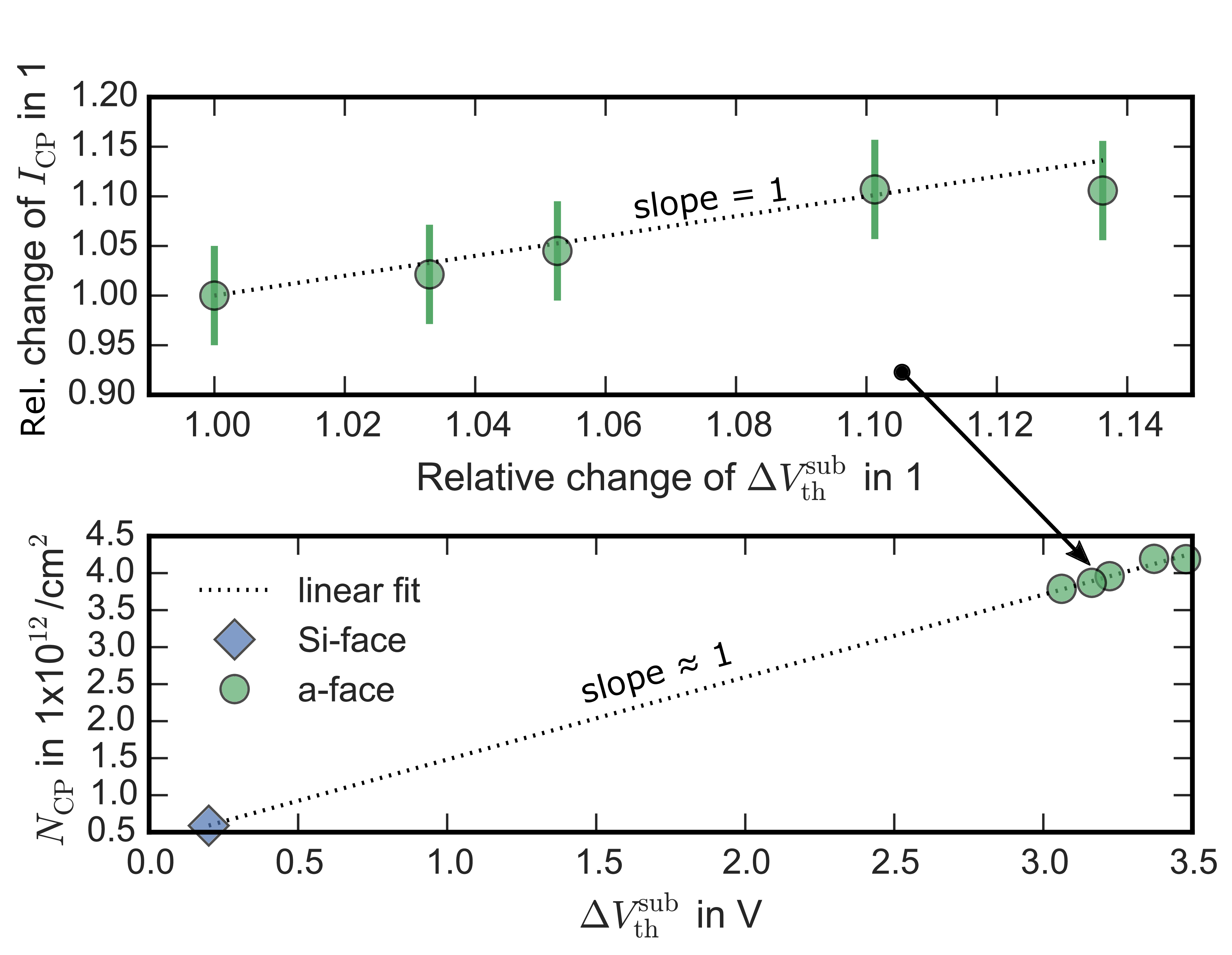
Figure 2.28: Top: linear increase of the charge pumping current with increasing sweep hysteresis  on a-face devices. Bottom: increase in the num-
ber of pumped charges per cycle with increasing hysteresis for the Si-face (diamonds,
blue) and a-face (circles, green). Due to the linear dependence of the hysteresis and the charge pumping signal, likely originates from deep states at the SiC-
SiO2 interface.
on a-face devices. Bottom: increase in the num-
ber of pumped charges per cycle with increasing hysteresis for the Si-face (diamonds,
blue) and a-face (circles, green). Due to the linear dependence of the hysteresis and the charge pumping signal, likely originates from deep states at the SiC-
SiO2 interface.
A comparison of the trap numbers extracted via charge pumping and the subthreshold hysteresis  is given in Tab. 2.1. Although the absolute numbers of trapped charges at the SiC/SiO2 interface differs for both measurement techniques (compare with Fig. 2.24), the same trend is observed. The linear correlation between and the charge pumping current for a-face devices is depicted in Fig. 2.28 (top). Here, data is extracted at 30 °C. Devices which show a 5 % increased hysteresis also show a 5 % increased . In the bottom plot of Fig. 2.28 the correlation of and for both crystal planes is depicted. Again, the
result suggests the same origin for the hysteresis and increased charge pumping current on both crystal faces. The reason for the diverging values for both extraction methods is explained in the next section.
is given in Tab. 2.1. Although the absolute numbers of trapped charges at the SiC/SiO2 interface differs for both measurement techniques (compare with Fig. 2.24), the same trend is observed. The linear correlation between and the charge pumping current for a-face devices is depicted in Fig. 2.28 (top). Here, data is extracted at 30 °C. Devices which show a 5 % increased hysteresis also show a 5 % increased . In the bottom plot of Fig. 2.28 the correlation of and for both crystal planes is depicted. Again, the
result suggests the same origin for the hysteresis and increased charge pumping current on both crystal faces. The reason for the diverging values for both extraction methods is explained in the next section.


2.6.1 Discrepancies between input characteristics and charge pumping
The discrepancy in the total number of trapped charges extracted via the sweep hysteresis and the charge pumping technique originates from the following facts:
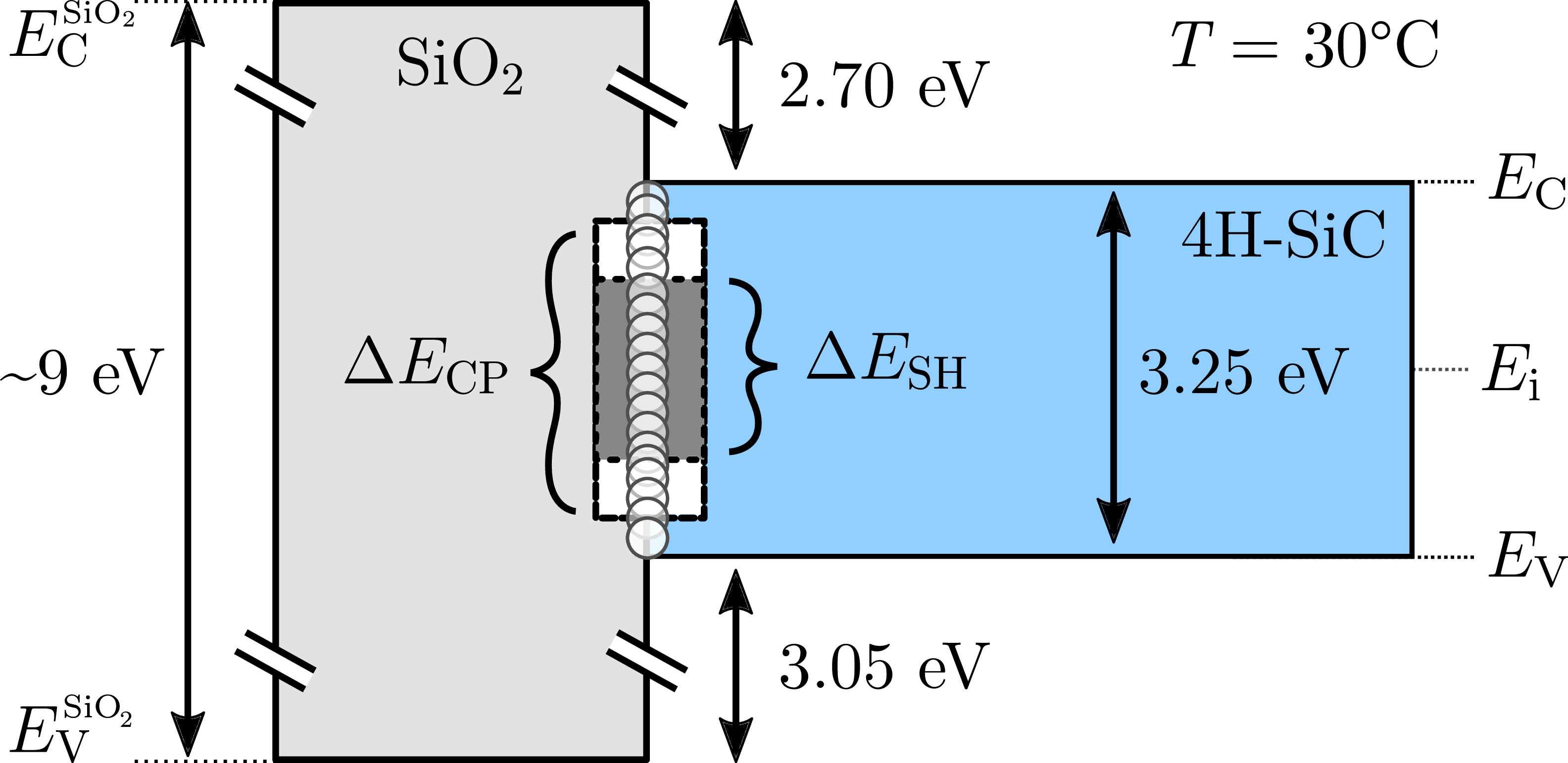
Figure 2.29: Schematic band diagram of the SiC-SiO2 system to illustrate the difference in the active energy window in the charge pumping and sweep hysteresis  measurements. Due to the slower
slew rates, is approximately 0.8 eV
narrower at 30 °C resulting in a reduced number of interface states, which contribute to the measurement signal.
measurements. Due to the slower
slew rates, is approximately 0.8 eV
narrower at 30 °C resulting in a reduced number of interface states, which contribute to the measurement signal.
-
• First,
extracted from the sweep hysteresis in our
measurements is read out via the drain current at  . Extracting at lower drain current, and therefore lower
inversion carrier density (see Section 2.3), will result in a higher (compare to Fig. 2.2). Due to this, extracted from the sweep hysteresis gives a
lower limit of the total interface trap density. To extract the total number of trapped charges one needs to read out the at infinitesimal small drain current, which is not
possible due to experimental limits of the measurement setup.
. Extracting at lower drain current, and therefore lower
inversion carrier density (see Section 2.3), will result in a higher (compare to Fig. 2.2). Due to this, extracted from the sweep hysteresis gives a
lower limit of the total interface trap density. To extract the total number of trapped charges one needs to read out the at infinitesimal small drain current, which is not
possible due to experimental limits of the measurement setup. -
• Second, the effective band gap energy window
scanned in the CP measurements is a function
of the gate voltage rise and fall times and is given by [87]with the Boltzmann constant
 , the temperature
  , the mean thermal velocity of holes and electrons
  , the mean capture
cross section of holes and electrons
, the mean capture
cross section of holes and electrons  , the intrinsic carrier density
  , the amplitude of the gate pulse
  , the charge pumping flatband and threshold
voltages
, the charge pumping flatband and threshold
voltages  and
and  and the rise and fall times of the gate pulse
 and
and  . In CP measurements, the gate voltage was
switched from the high level to the low level within hundreds of nanoseconds compared to the relatively slow gate level slew rate in the range of
. In CP measurements, the gate voltage was
switched from the high level to the low level within hundreds of nanoseconds compared to the relatively slow gate level slew rate in the range of  used in the the sweep
measurements. Due to the difference in the slew rate, one has to consider the following two effects:
used in the the sweep
measurements. Due to the difference in the slew rate, one has to consider the following two effects: -
(i) According to (2.14),
shrinks with decreasing rise time and fall time . Therefore, the energy window scanned in the
charge pumping measurements with a switching slope of  corresponds to
 whereas the energy window scanned in the sweep hysteresis measurements with a switching slope of
1 s/V corresponds to
whereas the energy window scanned in the sweep hysteresis measurements with a switching slope of
1 s/V corresponds to  at 30 °C. The difference in the active energy window is depicted in Fig. 2.29. The narrower energy range is due to the fast emission of
electrons close to the conduction band edge during the down sweep and due to the fast emission of holes close to the valance during the up-sweep. In total, 0.8 eV less than the SiC bandgap is electrically visible in the sweep
hysteresis measurement at 30 °C and therefore all trap states within these 0.8 eV do not contribute to the signal.
at 30 °C. The difference in the active energy window is depicted in Fig. 2.29. The narrower energy range is due to the fast emission of
electrons close to the conduction band edge during the down sweep and due to the fast emission of holes close to the valance during the up-sweep. In total, 0.8 eV less than the SiC bandgap is electrically visible in the sweep
hysteresis measurement at 30 °C and therefore all trap states within these 0.8 eV do not contribute to the signal. -
(ii) With decreasing
, , an increasing number of oxide or near interface
traps with longer time constants contribute to the signal. In our case, the effect on the sweep hysteresis in the subthreshold regime is in the range of millivolts and therefore negligible compared to the drift of several volts caused by
the high number of fast interface states.
-

2.6.2 Trap distributions using spectroscopic charge pumping
The discrepancy between mobility and  is a result of the different energetic distributions
of interface/border states for both crystal planes. The energetic distribution of was extracted using spectroscopic charge
pumping following the approach of van den Bosch [89]. A short introduction to the technique is given in Section 1.3.4. By varying the rise and fall times in addition to the measurement
temperature, the active energy window changes according to (2.14). Thereby one is able to scan a large fraction of the SiC band gap and calculate from the change in the charge pumping current.
Fig. 2.30 shows as a function of the rise time (triangles up) and
fall time (triangles down) of the gate pulse in a temperature range between −60 °C (blue) and 200 °C (red) for the Si-face device.
is a result of the different energetic distributions
of interface/border states for both crystal planes. The energetic distribution of was extracted using spectroscopic charge
pumping following the approach of van den Bosch [89]. A short introduction to the technique is given in Section 1.3.4. By varying the rise and fall times in addition to the measurement
temperature, the active energy window changes according to (2.14). Thereby one is able to scan a large fraction of the SiC band gap and calculate from the change in the charge pumping current.
Fig. 2.30 shows as a function of the rise time (triangles up) and
fall time (triangles down) of the gate pulse in a temperature range between −60 °C (blue) and 200 °C (red) for the Si-face device.
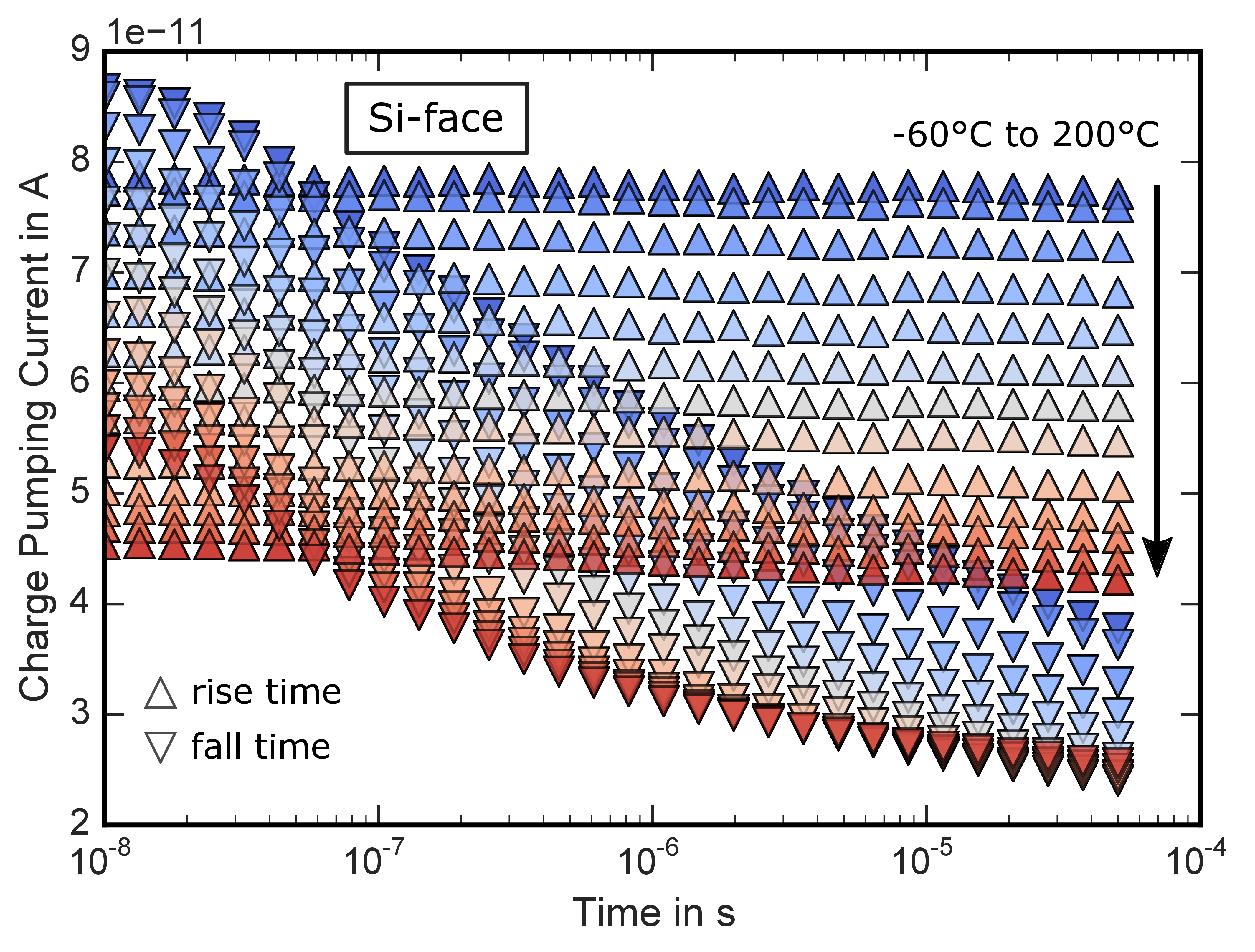
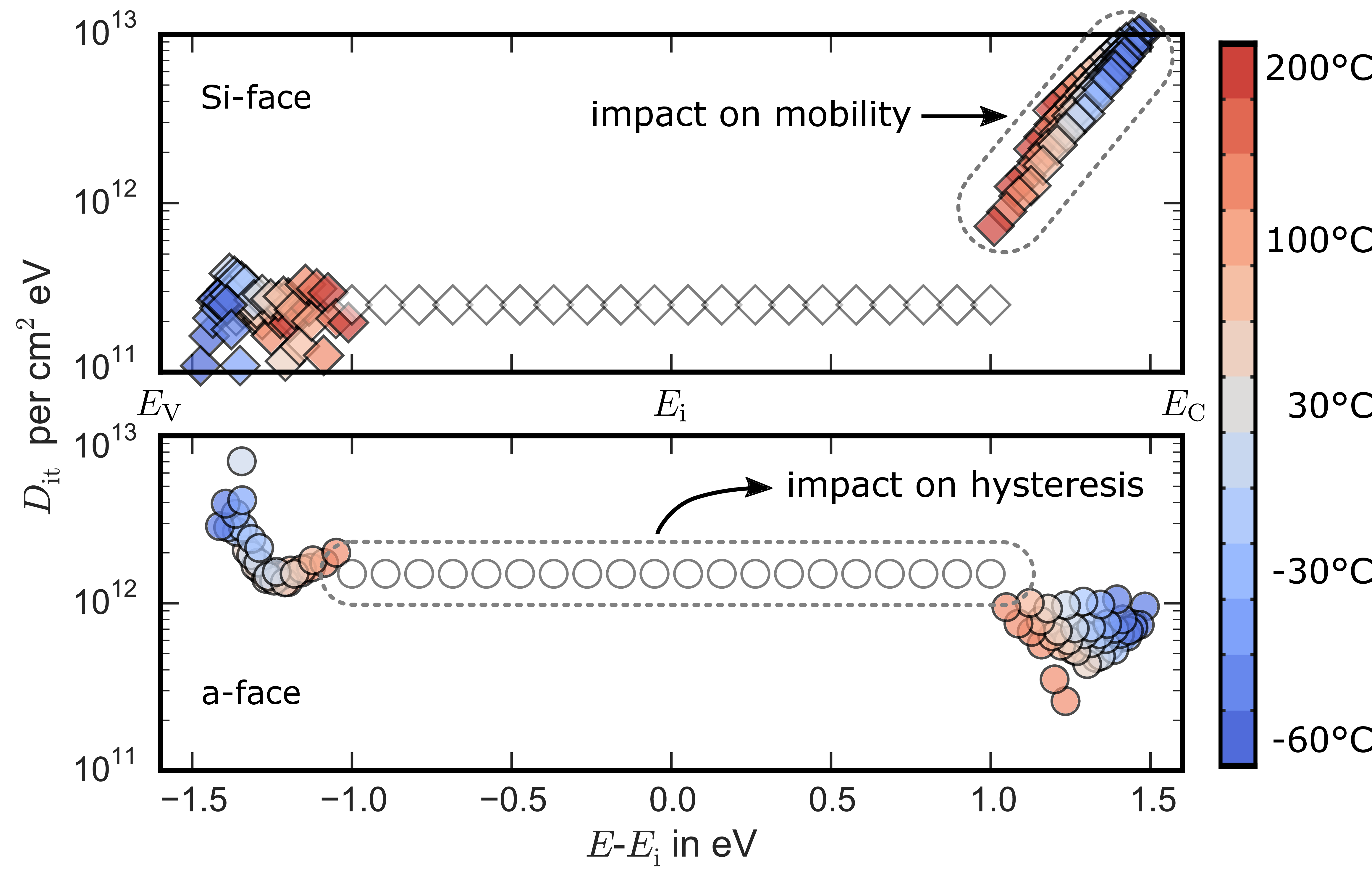
Figure 2.31: Energetic distribution of interface states for the Si-face (diamonds, top) and a-face (circles, bottom). Although the a-face shows 5 times higher around midgap resulting in a more pronounced
hysteresis, the close to  is about one order of magnitude lower resulting
in improved mobility. Note that for the a-face device, the points close to do not overlap. This is because most of the charge
pumping signal of the a-face device originates from deep states, which results in a very bad signal-to-noise ratio close to the band edges.
is about one order of magnitude lower resulting
in improved mobility. Note that for the a-face device, the points close to do not overlap. This is because most of the charge
pumping signal of the a-face device originates from deep states, which results in a very bad signal-to-noise ratio close to the band edges.
By calculating for every data point using (2.14), one is able to extract the energy distribution of traps, which contribute to the charge pumping signal. The outcome is shown in Fig. 2.31 for both crystal faces. Starting with the Si-face (top), one observes a of approximately  around mid-gap, which furthermore increases exponentially close to the conduction band edge of 4H-SiC, resulting in a bad mobility. The a-face device (bottom) shows an approximately 5 times higher
around mid-gap resulting in a more pronounced
subthreshold hysteresis, whereas the is much lower close to favoring higher mobility. The difference in
close to the conduction band edge for a-face and
Si-face devices annealed in nitric oxide (NO) is supported by the results of Kimoto et al. [117] who used the
around mid-gap, which furthermore increases exponentially close to the conduction band edge of 4H-SiC, resulting in a bad mobility. The a-face device (bottom) shows an approximately 5 times higher
around mid-gap resulting in a more pronounced
subthreshold hysteresis, whereas the is much lower close to favoring higher mobility. The difference in
close to the conduction band edge for a-face and
Si-face devices annealed in nitric oxide (NO) is supported by the results of Kimoto et al. [117] who used the  method, which is based on the
theoretical capacitance curve of the devices and does not give any information about states deep in the band gap.
method, which is based on the
theoretical capacitance curve of the devices and does not give any information about states deep in the band gap.
Previous: 2.5 Crystal face dependence Top: 2 On the first Component: the Subthreshold Hysteresis Next: 2.7 Possible atomic origin