« PreviousUpNext »Contents
Previous: 2.3 Gate voltage dependence Top: 2 On the first Component: the Subthreshold Hysteresis Next: 2.5 Crystal face dependence
2.4 Time and temperature dependence
As shown in Fig. 2.3, biasing the device in accumulation ( ) is sufficient to completely
charge the interface states and observe the maximum hysteresis. The positive charging of the interface states at this voltage level happens within several nanoseconds [111], and can therefore not be resolved due to the technical
limitations of our measurement setup. Due to this, the next sections focus on the time and temperature dependence of the recovery, assuming the interface is always completely positively charged, which will be the case after an
accumulation pulse longer than approximately 500 ns [111].
) is sufficient to completely
charge the interface states and observe the maximum hysteresis. The positive charging of the interface states at this voltage level happens within several nanoseconds [111], and can therefore not be resolved due to the technical
limitations of our measurement setup. Due to this, the next sections focus on the time and temperature dependence of the recovery, assuming the interface is always completely positively charged, which will be the case after an
accumulation pulse longer than approximately 500 ns [111].
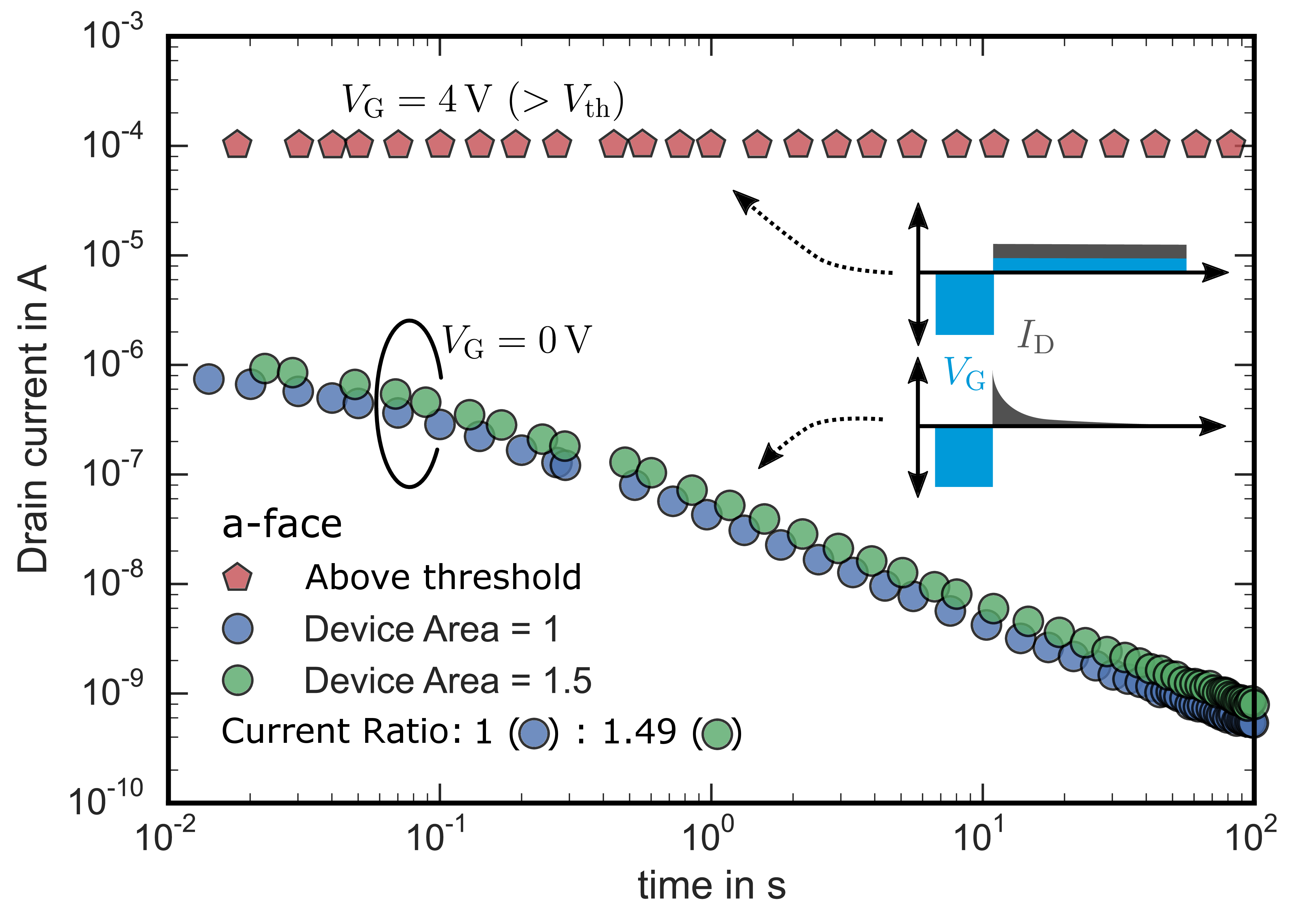
Figure 2.5: Recovery of the drain current at gate voltages below and above the threshold voltage after a charging pulse at for 1 s on an a-face
device. The same trend is observed on Si-face devices. The green data corresponds to a device with a 50 % increased active area. The measurement pattern is depicted in the inset.
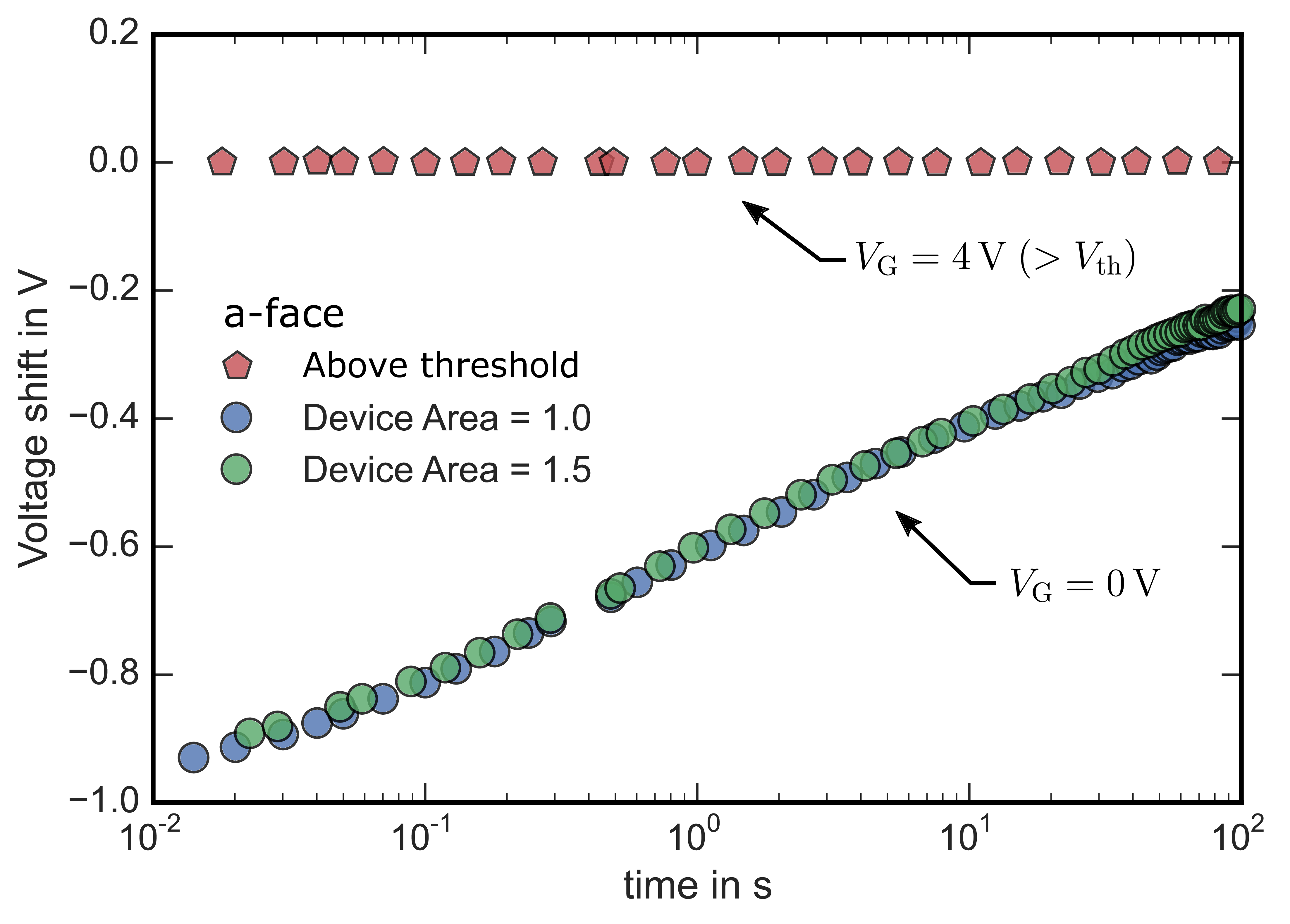
Figure 2.6: Voltage shift according to the recovery of the drain current in Fig. 2.5. The voltage shift is independent of the active area (circles) and disappears for gate voltages above the threshold voltage (red, pentagons) indicating a uniform distribution of the drain current over the entire active device area.
To analyze the time dependence of the hysteresis recovery, we start with the worst case scenario: a bias switch from strong accumulation with a completely positively charged interface to (a) the threshold voltage, or (b)
0 V. The outcome is shown in Fig. 2.5. For a bias switch from to  , which is slightly above the
threshold voltage. In this case,
, which is slightly above the
threshold voltage. In this case,  is stable over time (red, pentagons) and the
hysteresis has already fully recovered before the experimental time window, which starts 20 ms after the bias switch from to . On the other hand,
switching from to
is stable over time (red, pentagons) and the
hysteresis has already fully recovered before the experimental time window, which starts 20 ms after the bias switch from to . On the other hand,
switching from to  results in measurable drain
current transients due to the hysteresis effect (green and blue). Typically should be lower than
1 × 10⁻¹⁰ A at . However, due to the
negative shift of
results in measurable drain
current transients due to the hysteresis effect (green and blue). Typically should be lower than
1 × 10⁻¹⁰ A at . However, due to the
negative shift of  caused by trapped positive
charges, a drain current of approximately 1 µA is detected 20 ms after switching the bias from to . The drain current
transients are only visible due to the very slow detrapping of charges for Fermi level positions away from the SiC conduction band edge, which is the case for a gate voltage around 0 V.
caused by trapped positive
charges, a drain current of approximately 1 µA is detected 20 ms after switching the bias from to . The drain current
transients are only visible due to the very slow detrapping of charges for Fermi level positions away from the SiC conduction band edge, which is the case for a gate voltage around 0 V.
From Fig. 2.5 it is also clear that the hysteresis does not change with the active device area. This is proven via the green and blue data traces (circles), which
represent two a-face devices with different active area but otherwise identical. The drain current scales perfectly with device area indicating a uniform distribution of the current over the whole device. The corresponding voltage shift
at is shown in Fig. 2.6 and is identical for both devices. This proves that the hysteresis is not due to a local device leakage current caused by localized electric field variations, which
might for example occur at the edges of the device, but is uniformly distributed over the entire active device area. The voltage shift at recovers slowly with
approximately 175 mV per decade in time. Detrapping until the drain current falls below the measurable window takes at least 1000 s.
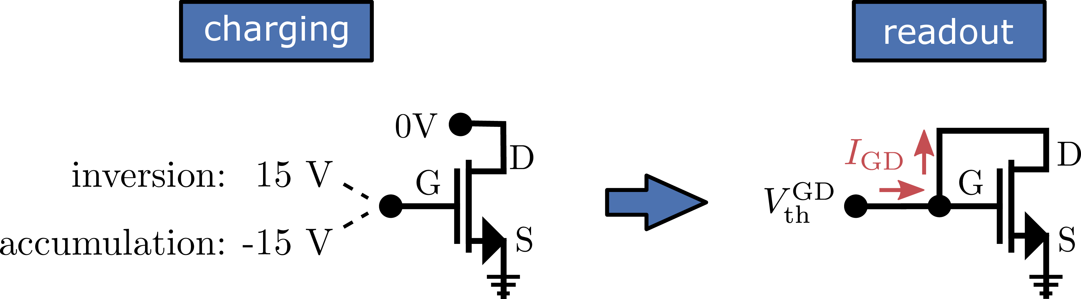
Figure 2.7: Measurement schematics for the extraction of the hysteresis using a gated diode circuit. The gate is either charged in strong-inversion (15 V) or in accumulation ( ) for a charging time of 1 s with
grounded source and drain terminals (left). Afterwards,
) for a charging time of 1 s with
grounded source and drain terminals (left). Afterwards,  or
or  , respectively, is extracted by
forcing various current levels
, respectively, is extracted by
forcing various current levels  using the gated diode circuit with the drain con-
nected to the gate contact.
using the gated diode circuit with the drain con-
nected to the gate contact.
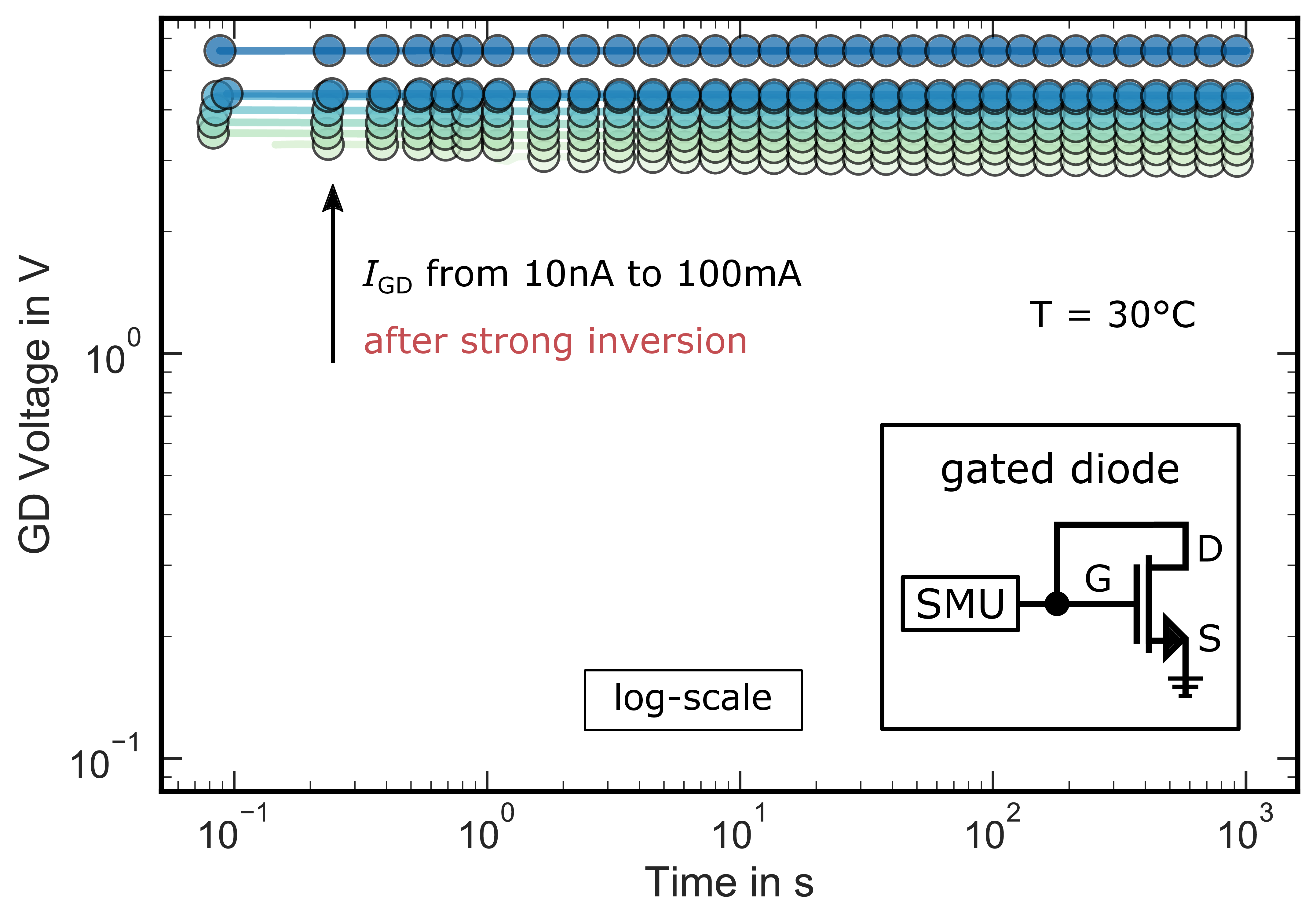
Figure 2.8: Gated-diode voltage at various current levels ranging from 10 nA to 100 mA
for 1000 s after charging the gate in strong-inversion at 15 V for 1 s. is nearly stable within the
measurement window. All traces have been recorded using a gated diode circuit, which shorts the gate and drain contacts of the devices as indicated in the inset.
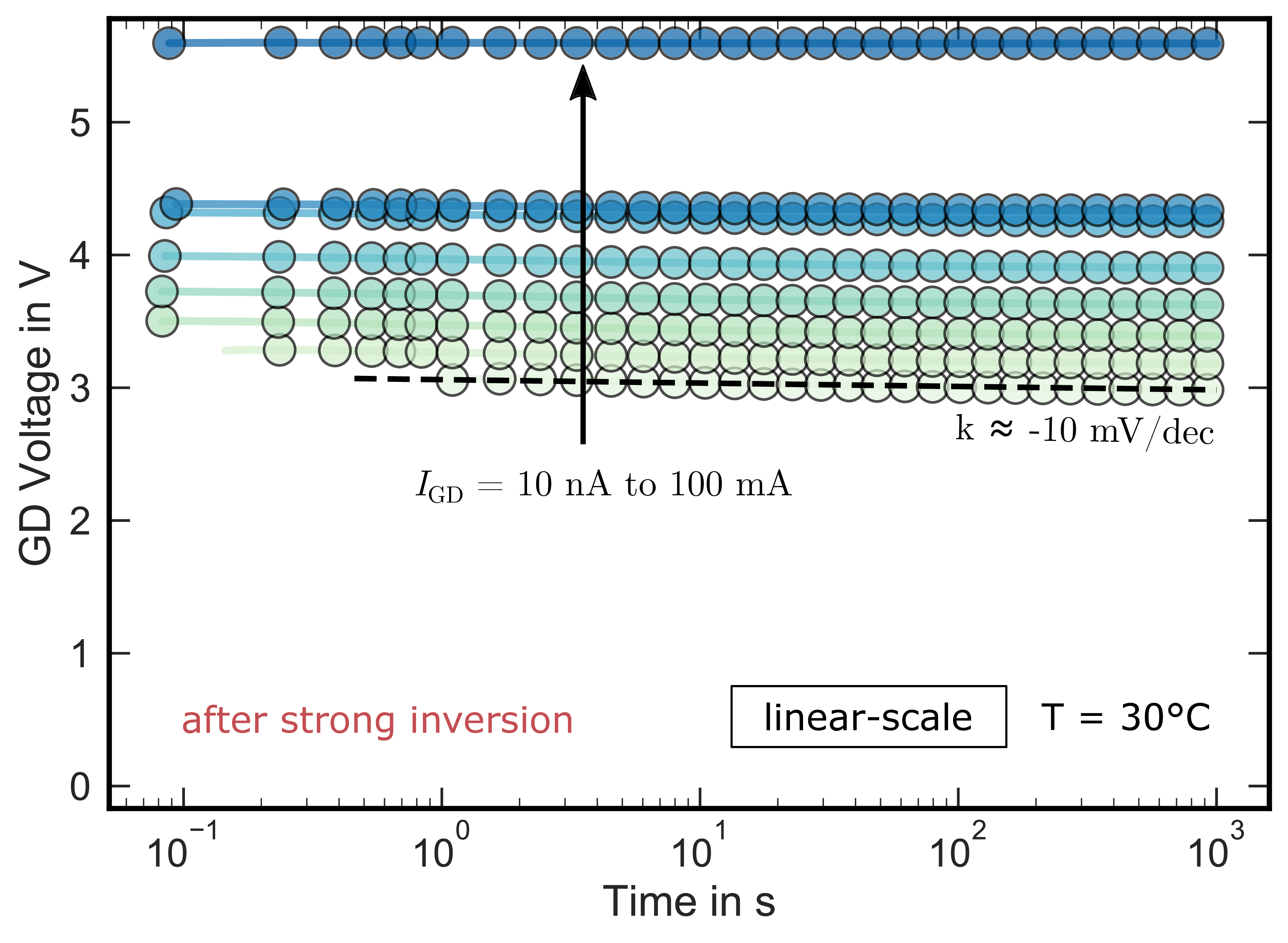
Figure 2.9: Same as Fig. 2.8 but now with linear y-scale. Only a small remaining recovery slope of approximately  dec
is visible due to charge emission form trap states, which captured an electron during the preceding inversion pulse.
dec
is visible due to charge emission form trap states, which captured an electron during the preceding inversion pulse.
2.4.1 Hysteresis after strong inversion
Before we discuss the more complicated hysteresis effect after an accumulation pulse in more detail, we start by analyzing the threshold voltage instability after a positive bias pulse above threshold (inversion). In this case, the
gate bias is switched from strong inversion to a fixed readout current at which  is extracted.
Here, the superscript GD indicates that a gated-diode circuit is used for the readout of the threshold voltage to keep the
inversion carrier density in the channel constant during the readout. The stress/measurement schematics are shown in Fig. 2.7. At first, the interface is
charged in strong inversion at
is extracted.
Here, the superscript GD indicates that a gated-diode circuit is used for the readout of the threshold voltage to keep the
inversion carrier density in the channel constant during the readout. The stress/measurement schematics are shown in Fig. 2.7. At first, the interface is
charged in strong inversion at  for 1 s while the
source and drain terminals are grounded (left). Afterwards, the connection scheme is changed to the gated diode configuration using a switching matrix and a current is forced at the shorted drain/gate terminals
while the corresponding voltage at these terminals, , is monitored. Note that no
gate-leakage current flows if a current is forced during the gated-diode configuration.
Instead, the potential at the gate terminal rises until the inversion channel forms. From this point on, the forced flows exclusively from drain to source, as
indicated by the red arrows in Fig. 2.7.
for 1 s while the
source and drain terminals are grounded (left). Afterwards, the connection scheme is changed to the gated diode configuration using a switching matrix and a current is forced at the shorted drain/gate terminals
while the corresponding voltage at these terminals, , is monitored. Note that no
gate-leakage current flows if a current is forced during the gated-diode configuration.
Instead, the potential at the gate terminal rises until the inversion channel forms. From this point on, the forced flows exclusively from drain to source, as
indicated by the red arrows in Fig. 2.7.
Fig. 2.8 and Fig. 2.9 shows the transients in logarithmic
and linear y-scale at various forced current levels ranging from 10 nA to
100 mA for 1000 s. is immediately stable
within our measurement window. Only a small remaining recovery slope of approximately dec is visible due to charge emission from border/oxide traps, which captured an electron during the preceding strong inversion pulse. This behavior is the typical voltage recovery, which occurs after
positive bias stress as will be discussed in more detail in Chap. 3. A basic overview is provided in Section 3.
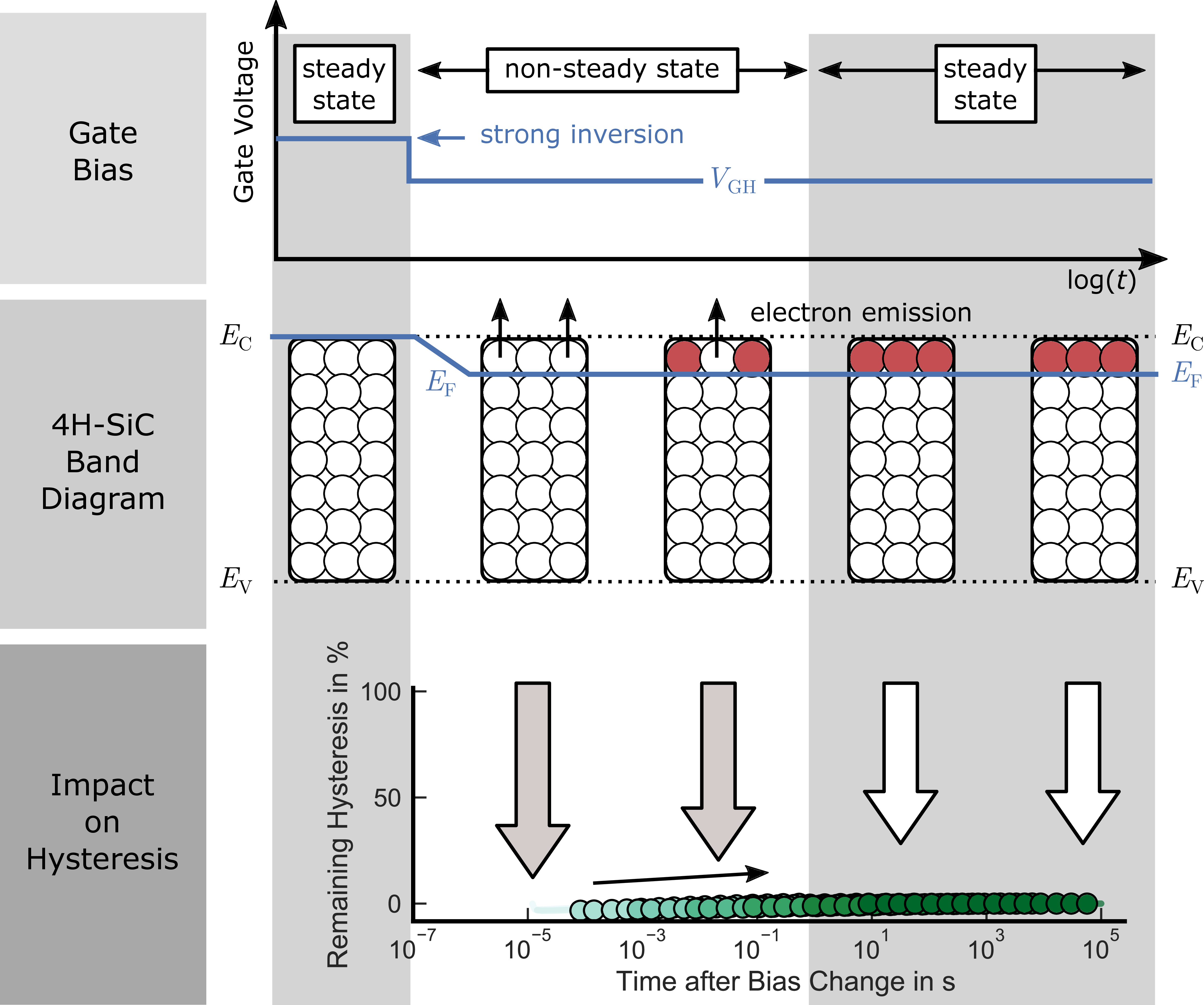
Figure 2.10: Schematic illustration of the interface charging state after switching the gate bias from strong inversion to inversion. The change in gate voltage is indicated at the top. The observed instability (bottom) is mainly defined by electron emission from trap states close to the conduction band edge (middle).
The interface trap charging state after the bias change from strong inversion to is sketched in Fig. 2.10. The bias switch is indicated at the top, the interface charge state in the middle and the observed relative hysteresis at the bottom. After the bias switch, the
Fermi level changes only slightly and remains close to the conduction band edge. Assuming only interface states, the time constant for electron emission  according to Shockley-Read-Hall (SRH) [112, 113]
is given by
according to Shockley-Read-Hall (SRH) [112, 113]
is given by

with the thermal velocity for electrons  , the capture cross section
  and the effective density of states in the
conduction band
and the effective density of states in the
conduction band  . After the bias switch from strong inversion to
inversion,
. After the bias switch from strong inversion to
inversion,  remains close to
  and thermal equilibrium is restored almost
immediately by electron emission from trap states above the Fermi level to (Fig. 2.10, middle) resulting in a stable, hysteresis free, drain current (Fig. 2.10, bottom). Note that
no hole capture occurs because the interface remains inverted.
and thermal equilibrium is restored almost
immediately by electron emission from trap states above the Fermi level to (Fig. 2.10, middle) resulting in a stable, hysteresis free, drain current (Fig. 2.10, bottom). Note that
no hole capture occurs because the interface remains inverted.
The remaining recovery slope of approximately dec originates from border trap states with broadly distributed emission time constants, which can be described according to (1.6) (see Section 1.2.1). These states will be intensively investigated
in Chap. 3.
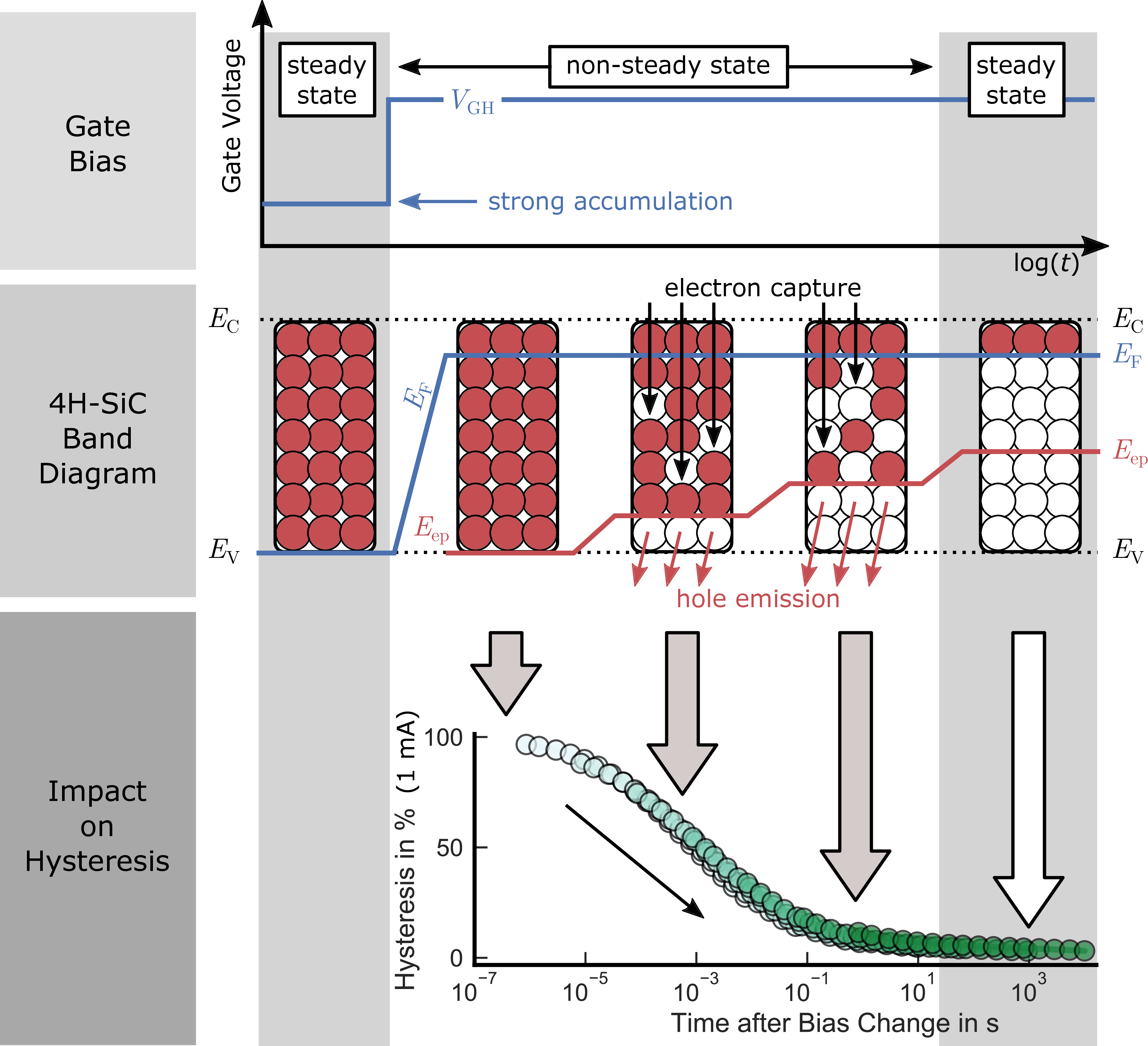
Figure 2.11: Schematic illustration of the interface charging state after switching the gate bias from accumulation to inversion. Top: timing of the gate voltage. Middle: after the 1 s accumulation pulse, the interface is fully positively charged. Bottom: after switching to inversion, more and more positive charge is lost via hole emission and electron capture leading to a decrease a recovery of the hysteresis.
2.4.2 Hysteresis after accumulation
In contrast to the behavior after charging the interface in strong inversion, the outcome changes drastically if the device is charged via an accumulation pulse. The switching process is sketched in Fig. 2.11 with the voltage level at the gate contact (top), the interface charging state (middle), and the relative hysteresis (bottom). Starting in accumulation, where the
Fermi level is pinned to the valence band, the interface is assumed to be positively charged and in thermal equilibrium. After switching to inversion, where  is measured, the Fermi level crossed nearly the
entire SiC band gap, which results in a non-steady interfacial charge state. Thermal equilibrium is slowly restored by
is measured, the Fermi level crossed nearly the
entire SiC band gap, which results in a non-steady interfacial charge state. Thermal equilibrium is slowly restored by
-
• electron capture from the SiC conduction band, with time constants according to
with the inversion charge density
 ,
, -
• and hole emission to the SiC valence band edge
 , which follows
 with the thermal velocity
 and capture cross section of holes, and the effective density of states in
the valence band
and capture cross section of holes, and the effective density of states in
the valence band  [112, 113].


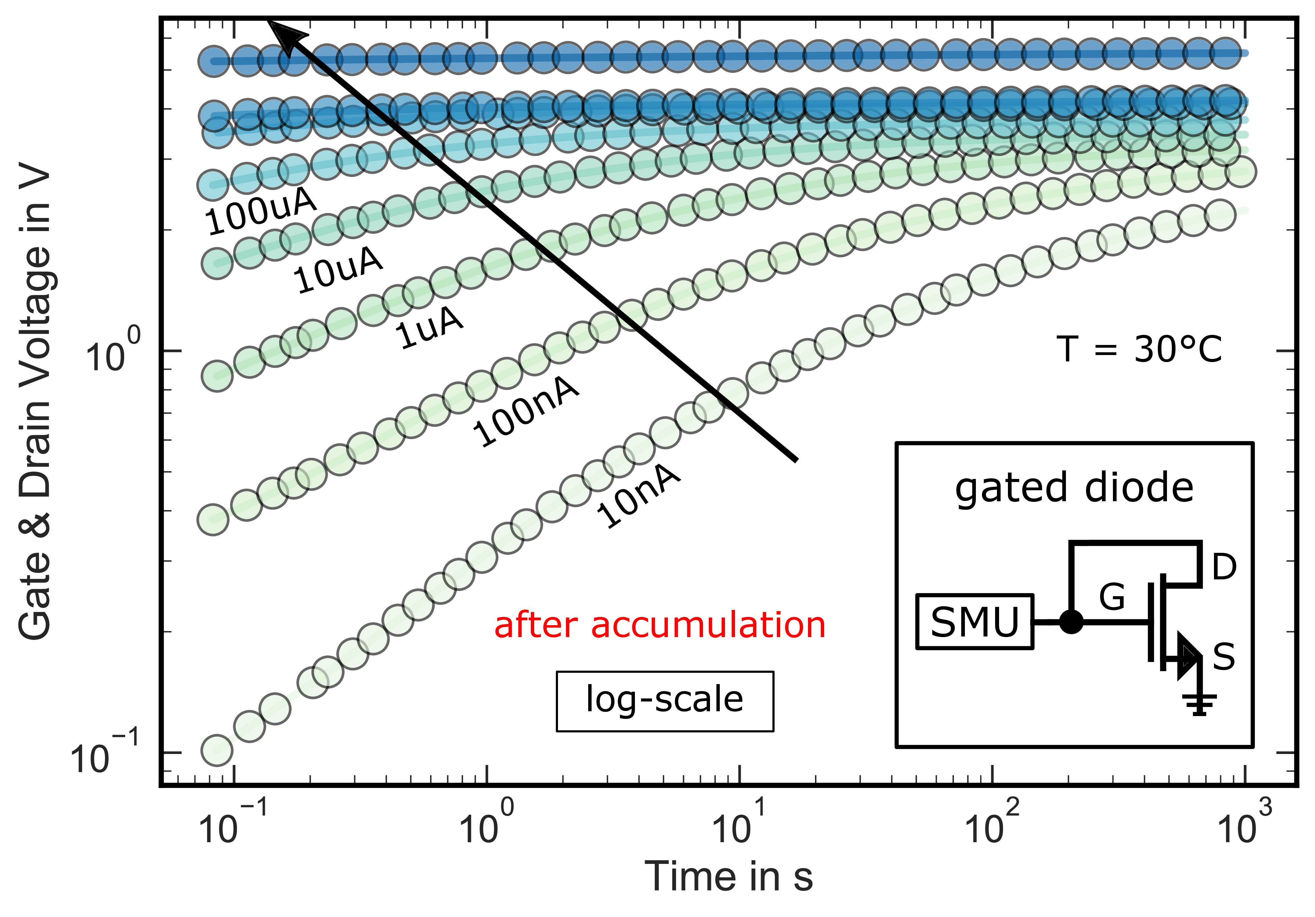
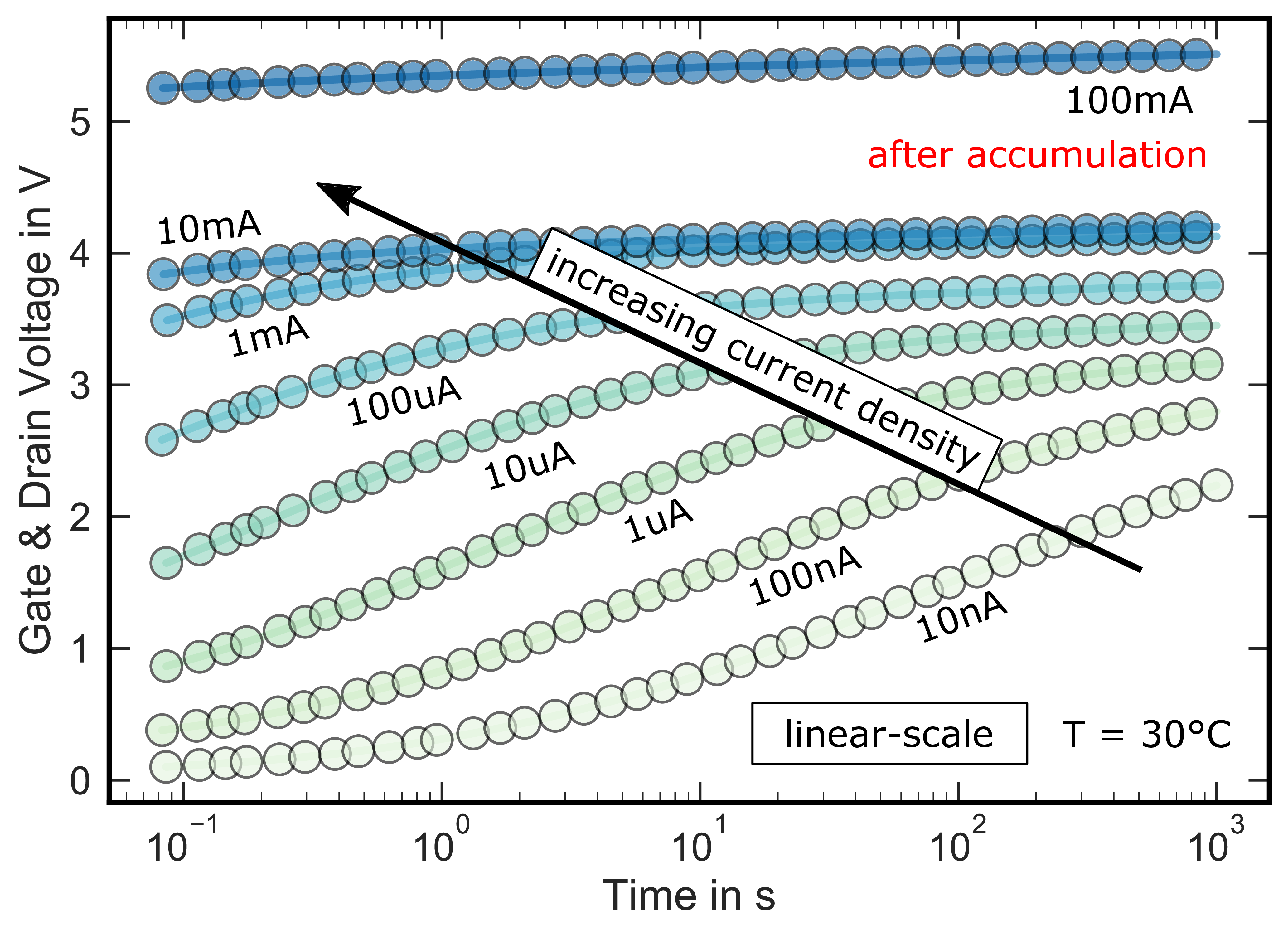
Figure 2.13: Same as Fig. 2.12 but now with linear y-scale. Recovery of the subthreshold hysteresis scales with current density.
Since hole emission is independent of the Fermi level according to (2.7), the main contribution to the restoration of thermal
equilibrium originates from electron capture according to (2.6). Therefore, the larger the inversion charge density (and thereby the gate voltage), the faster
thermal equilibrium is reached. Fig. 2.12 and Fig. 2.13 show for various inversion charge
densities. As before, the measurement is performed according to the schematics sketched in Fig. 2.8. Instead of a strong-inversion pulse, an accumulation
pulse at  is applied for 1 s.
After the charging pulse, ranging 10 nA to 10 mA is
forced using the gated diode circuit, while the corresponding gate/drain voltage (labeled as ) is monitored. From (2.6) and the fact that the drain current is to first order a direct measurement for via the textbook formula
is applied for 1 s.
After the charging pulse, ranging 10 nA to 10 mA is
forced using the gated diode circuit, while the corresponding gate/drain voltage (labeled as ) is monitored. From (2.6) and the fact that the drain current is to first order a direct measurement for via the textbook formula

it is obvious that the time to restore thermal equilibrium should be indirectly proportional to , if mainly interface states are responsible for the
hysteresis. This is in fact the case, as will be shown within the next sections.


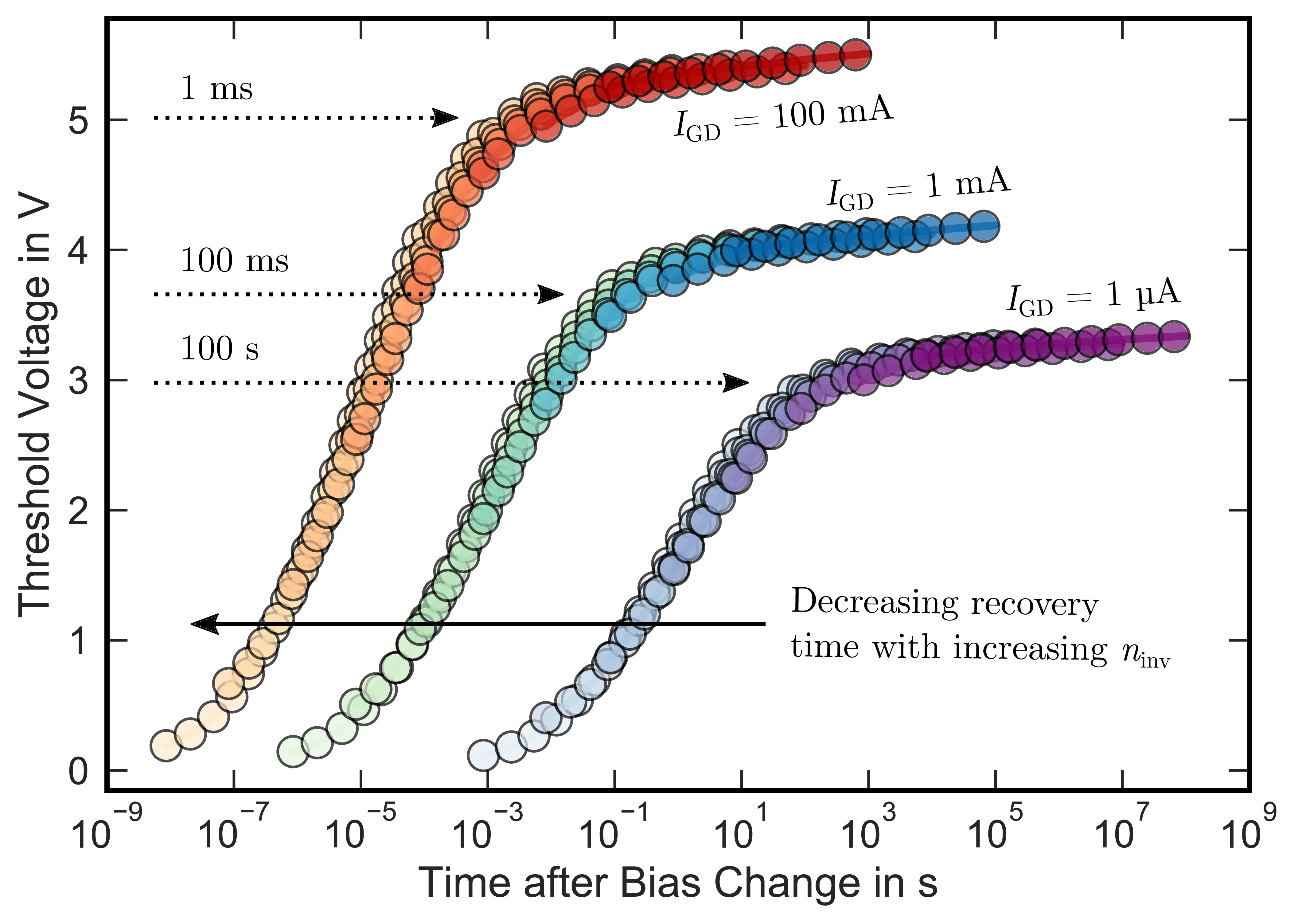
Figure 2.15: Universal recovery curves for a readout current of 0.1 A (red), 1 mA (green), and 1 µA (purple). The recovery time scales linearly with the inversion carrier density . For  (blue), the re-
covery time is approximately 100 ms, whereas for the 100 times higher current of
(blue), the re-
covery time is approximately 100 ms, whereas for the 100 times higher current of  , the recovery
time is 100 times shorter and approximately 1 ms (red).
, the recovery
time is 100 times shorter and approximately 1 ms (red).


The universal hysteresis recovery curve
If the recovery time constants of the hysteresis mainly scales with the free inversion carrier density , an increase of by a fixed factor should decrease the recovery
time constant by exactly the same factor according to (2.6). This is in fact true, since we are able to scale all transients from Fig.
2.12 onto a single universal recovery time  at any given readout current
 , by assuming to scale according to

Here,  is the time at the current level
, and
is the time at the current level
, and  and
and  the channel resistance at and , respectively.
Using the data from Fig. 2.12, all distinct transients can be transformed onto one universal recovery curve, which allows to extract the time to reach
thermal equilibrium at any given inversion carrier density represented by . Fig. 2.14 shows the universal recovery curve for a drain current of  . Coming from
strong accumulation, it takes about 100 ms until thermal equilibrium is restored and the corresponding gate voltage of 4 V to be stable. Fig. 2.15
shows the same curve for
. Coming from
strong accumulation, it takes about 100 ms until thermal equilibrium is restored and the corresponding gate voltage of 4 V to be stable. Fig. 2.15
shows the same curve for  ,
1 mA and 1 µA. Since we are able to describe the time constants solely via the SRH model, the recovery time scales linearly with the drain current, meaning a 100 times higher drain current corresponds to
2 orders of magnitude faster recovery time constants. This is proven in Fig. 2.15: at 1 mA, the time to reach thermal equilibrium is approximately
100 ms, whereas for a 100 times higher drain current of 100 mA thermal equilibrium is reached in 1 ms, which is exactly 100 times faster. The same is true for a 1000 times lower current of
1 µA (purple).
,
1 mA and 1 µA. Since we are able to describe the time constants solely via the SRH model, the recovery time scales linearly with the drain current, meaning a 100 times higher drain current corresponds to
2 orders of magnitude faster recovery time constants. This is proven in Fig. 2.15: at 1 mA, the time to reach thermal equilibrium is approximately
100 ms, whereas for a 100 times higher drain current of 100 mA thermal equilibrium is reached in 1 ms, which is exactly 100 times faster. The same is true for a 1000 times lower current of
1 µA (purple).
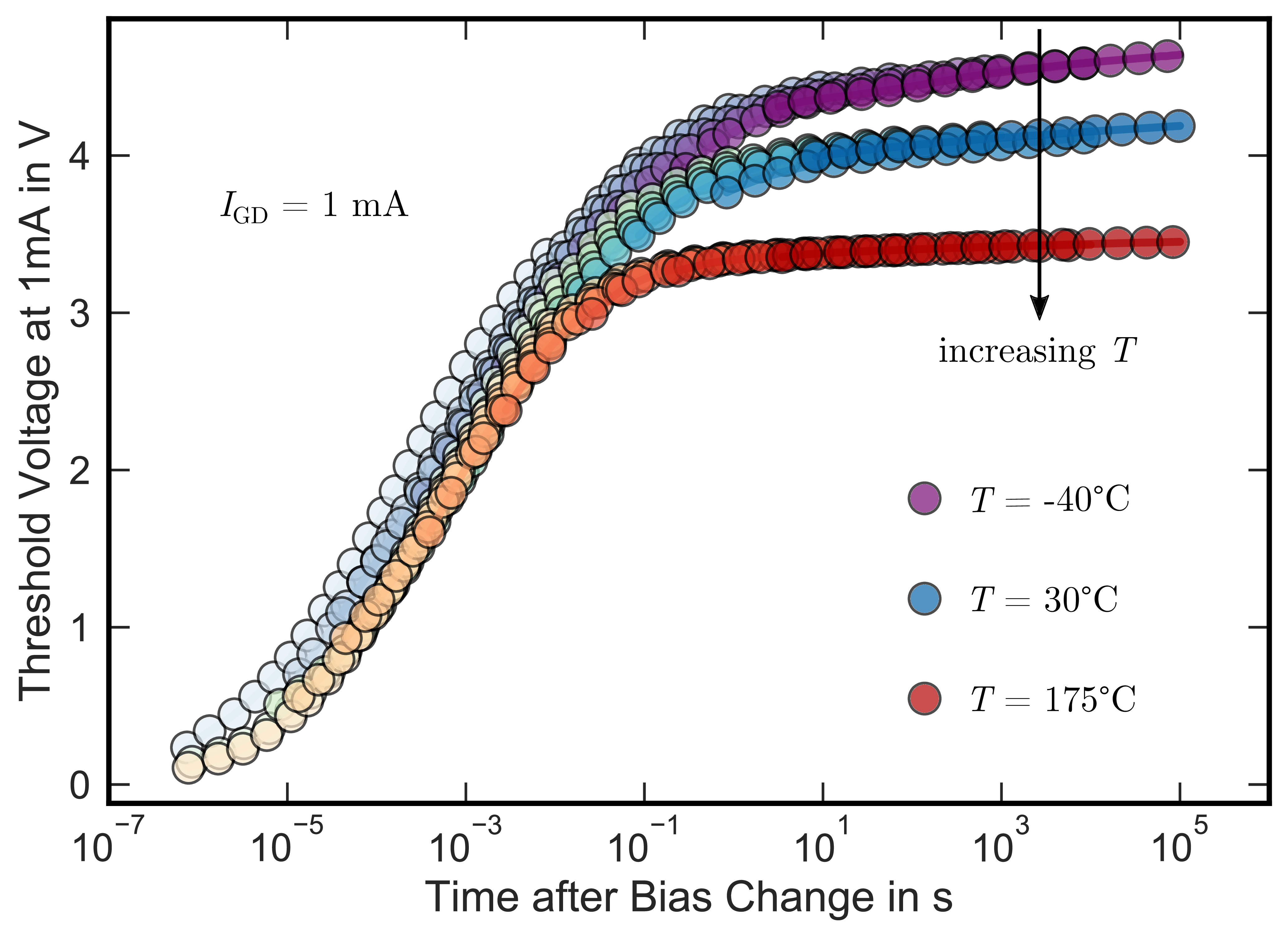
The temperature dependence of the universal recovery at is shown in
Fig. 2.16 for temperatures of −40 °C, 30 °C and 175 °C. As can be seen, the steady state  decreases from 4.8 V to approximately 3.5 V with increasing temperature. Interestingly, there seems to be ongoing recovery at −40 °C and 30 °C for times
 , as can be seen in the remaining
slopes of both curves. In general, one would attribute such a behavior to broadly distributed recovery time constants, which are hard to explain using a SRH based model. However, it will be shown in the next section that the
ongoing recovery "tail" can be attributed to broadly distributed NBTI recovery and therefore decoupled from the hysteresis effect.
, as can be seen in the remaining
slopes of both curves. In general, one would attribute such a behavior to broadly distributed recovery time constants, which are hard to explain using a SRH based model. However, it will be shown in the next section that the
ongoing recovery "tail" can be attributed to broadly distributed NBTI recovery and therefore decoupled from the hysteresis effect.
Distribution of recovery times
To extract the recovery time distribution of the interface states responsible for the hysteresis, first one has to disentangle the recovery signal from the convolution of fast states and the broadly distributed NBTI states. Fortunately,
this is easily possible due to the broadly distributed emission times of border states after positive and negative bias stress, as was for example shown in Fig. 2.9
after positive bias temperature stress (PBTS) with a constant slope of approximately  over the
whole measurement window.
over the
whole measurement window.
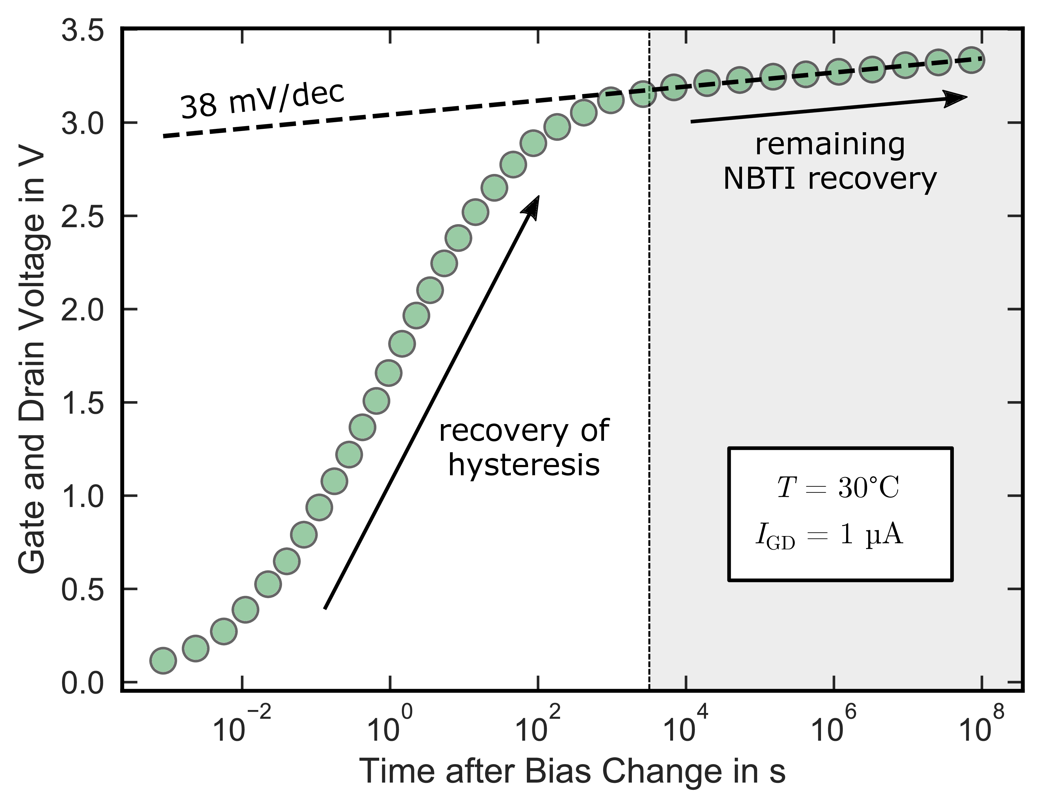
Figure 2.17: Convolution of the hysteresis recovery curve for a readout current of  . In addition to
the recovery of fast states (white background), a minor contribution originates from border states with broadly distributed time constants (NBTI recovery). The NBTI recovery component becomes dominant after the hysteresis is fully
recovered (gray background).
. In addition to
the recovery of fast states (white background), a minor contribution originates from border states with broadly distributed time constants (NBTI recovery). The NBTI recovery component becomes dominant after the hysteresis is fully
recovered (gray background).
The convolution of the hysteresis recovery curve for a readout current of is shown in
Fig. 2.17. In addition to the dominant recovery component of the fast interface states responsible for the hysteresis, an additional NBTI recovery component
is present, which becomes dominant at approximately 3 × 10³ s after the bias switch. Fortunately, the NBTI component is broadly distributed in time and therefore easy to remove from the hysteresis recovery
curve using a constant exponent  (cf. (1.3)), which allows for an explicit extraction of the recovery time distribution.
After the subtraction of the NBTI recovery, the recovery time  of the hysteresis can be fitted using a
log-normal distribution with the cumulative distribution function (CDF)
of the hysteresis can be fitted using a
log-normal distribution with the cumulative distribution function (CDF)

with the error function erf, and the parameters of the log-normal distribution  and
and  that are, respectively, the mean and standard
deviation of the normal distribution of
that are, respectively, the mean and standard
deviation of the normal distribution of  . The outcome for the universal
recovery curve at and
30 °C is shown in Fig. 2.18 (top). After the NBTI correction, the hysteresis recovery curve shows very good agreement with the log-normal
CDF with
. The outcome for the universal
recovery curve at and
30 °C is shown in Fig. 2.18 (top). After the NBTI correction, the hysteresis recovery curve shows very good agreement with the log-normal
CDF with  and
and  (dashed line). The resulting
probability density function (PDF) represents the distribution of the recovery time and is shown in the bottom plot in Fig. 2.18.
(dashed line). The resulting
probability density function (PDF) represents the distribution of the recovery time and is shown in the bottom plot in Fig. 2.18.
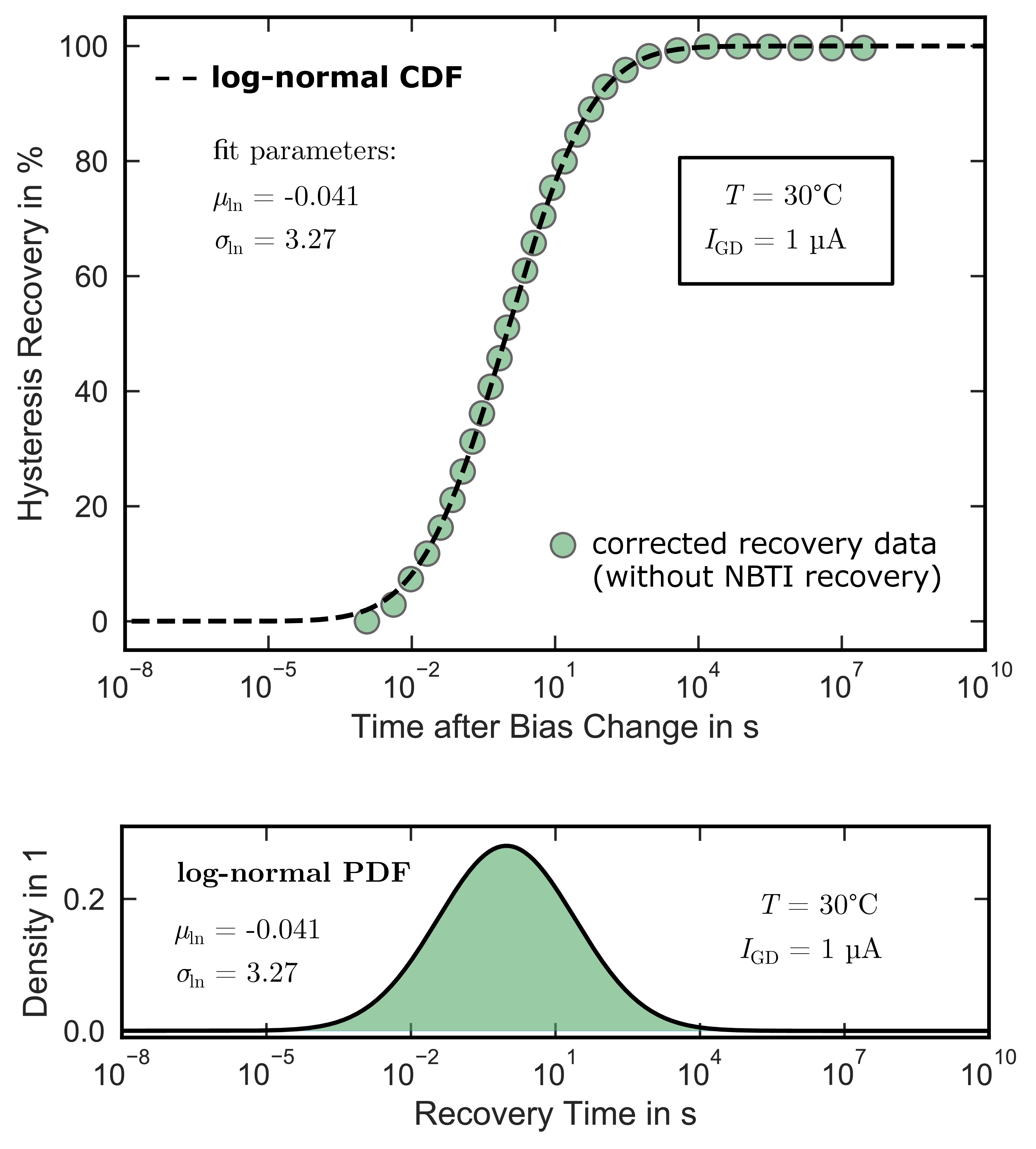

Fig. 2.19 shows the log-normal PDFs for  (blue),
  (green) and
  (red) at a current density of . The
parameter is independent of the temperature and varies
only slightly. Due to this, the recovery mechanism seems not to be temperature activated, or at least has an activation energy which is significantly below 100 meV. On the other hand, the distribution broadens for decreasing
temperatures, which results in slightly longer recovery times for lower temperatures. The dependence of the parameters of the log-normal distribution, and , on and
(red) at a current density of . The
parameter is independent of the temperature and varies
only slightly. Due to this, the recovery mechanism seems not to be temperature activated, or at least has an activation energy which is significantly below 100 meV. On the other hand, the distribution broadens for decreasing
temperatures, which results in slightly longer recovery times for lower temperatures. The dependence of the parameters of the log-normal distribution, and , on and  is shown in Fig. 2.20. As already mentioned, is nearly independent of but scales strongly with the inversion carrier density (see Fig. 2.20, left), which is proportional to . The median of the distribution
  , which is represented by the
parameter according to
, which is represented by the
parameter according to

decreases linearly with the logarithm of with a slope of  . On the other
hand, the standard deviation is not affected by (not shown), but increases with decreasing
with a slope of
. On the other
hand, the standard deviation is not affected by (not shown), but increases with decreasing
with a slope of  leading to a stretch out of the recovery time distribution for lower temperatures (Fig. 2.20, right).
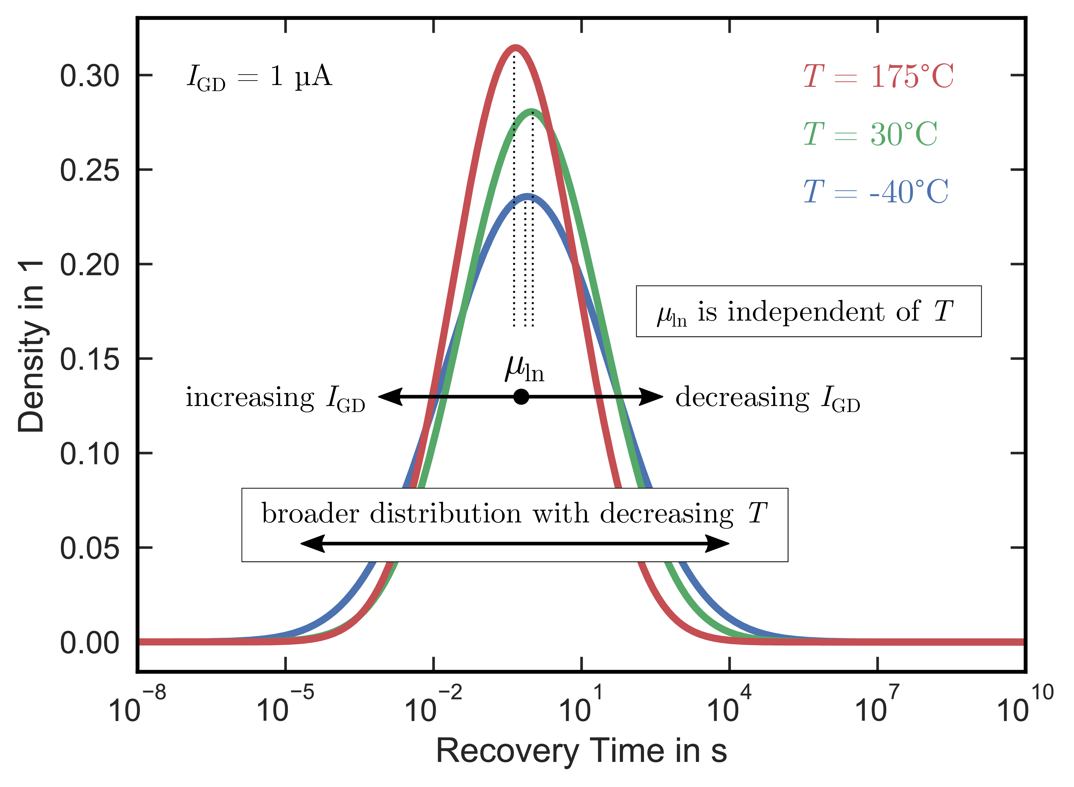
Figure 2.20: Parameters for the log-normal distribution of the hysteresis recovery times. Left: the parameter seems to be independent of and scales linearly with  with a slope of approximately
  . Right: the standard devi-
ation is independent of but seems to increase with decreasing , which indicates a broadening of the recovery time distribution for lower tempera-
tures.
. Right: the standard devi-
ation is independent of but seems to increase with decreasing , which indicates a broadening of the recovery time distribution for lower tempera-
tures.
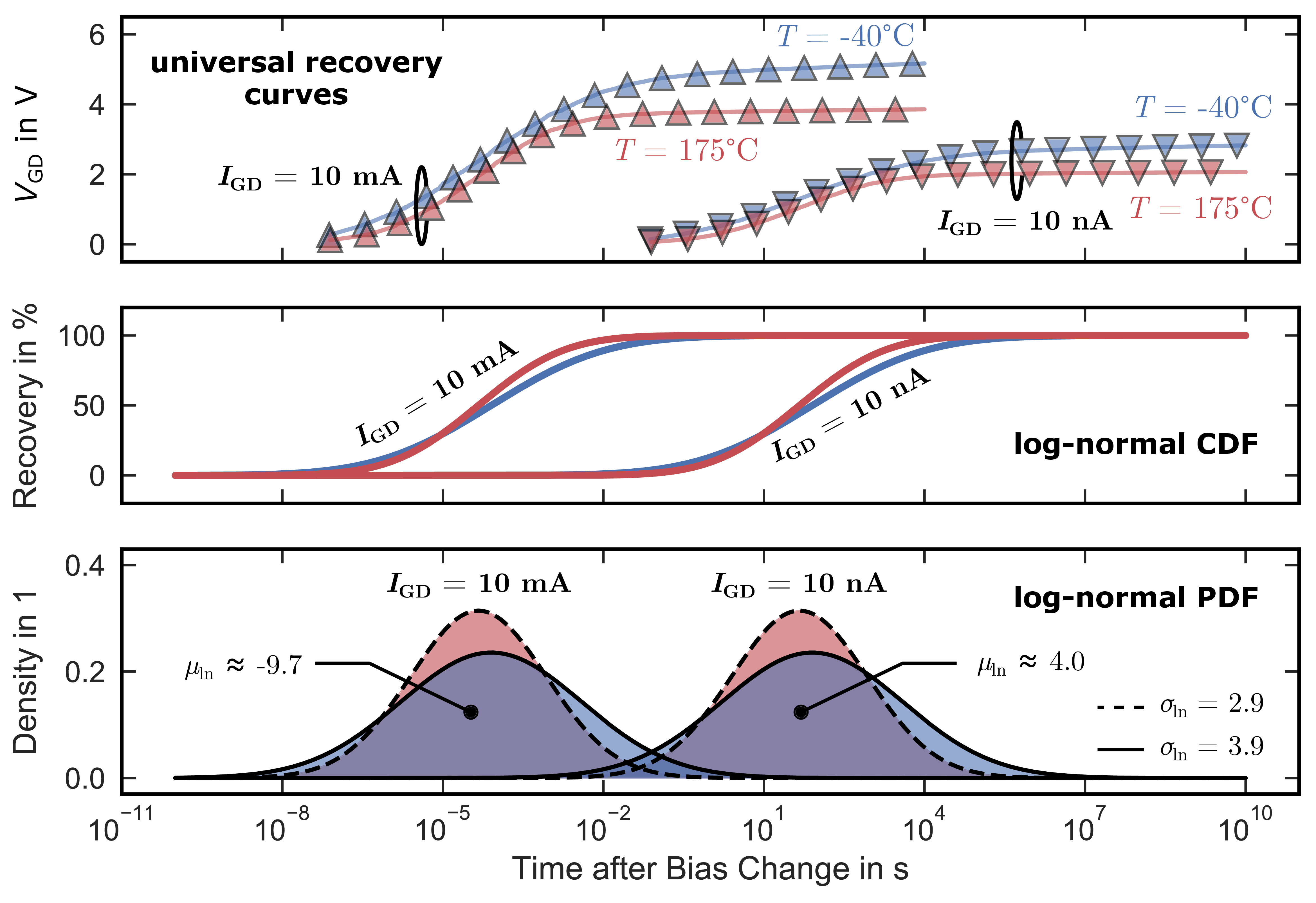
Figure 2.21: Recovery of the hysteresis as a function of the temperature for (blue) and (red) for  (right) and a 1
million times higher current density of
(right) and a 1
million times higher current density of  (left). Top:
universal recovery curves including the NBTI component, which is more pronounced for lower temperatures. Middle: log-normal cumulative distribution functions of the universal hysteresis curves corrected for NBTI recovery.
Bottom: probability density functions of the recovery times. For the
(left). Top:
universal recovery curves including the NBTI component, which is more pronounced for lower temperatures. Middle: log-normal cumulative distribution functions of the universal hysteresis curves corrected for NBTI recovery.
Bottom: probability density functions of the recovery times. For the  times higher current density (left), parameter decreases from
  to
to  for both temperatures, which
represents a times faster recovery time. On the other hand, the standard deviation increases from
for both temperatures, which
represents a times faster recovery time. On the other hand, the standard deviation increases from
 at to
at to  at with decreasing tem-
perature. This means the recovery time distribution broadens with lower and full recovery takes slightly longer.
at with decreasing tem-
perature. This means the recovery time distribution broadens with lower and full recovery takes slightly longer.
Figure 2.22: Time after bias change after which 95 % of the hysteresis is recovered for temperatures of (blue), (green) and (red) and current densities ranging from to . Top: proba-
bility density functions. Here the distributions for a current density of are highlighted,
whereas the PDFs for lower current densities are outlined only (dashed). Bottom: recovery time for 95 % recovery as a function of the temperature for various current densities.
Fig. 2.21 gives a final overview on the recovery of the hysteresis as a function of the temperature for (blue) and (red) for two different current densities of (right) and a
1 million times higher current density of (left). Fig.
2.21, top, shows the universal recovery curves, still including the NBTI component. As stated before, this component is more distinct for lower temperates, as
can be seen in the higher slope after the majority of the hysteresis is already recovered. After the NBTI component is removed, the relative amount of recovery can be extracted, which is represented by the CDF (Fig. 2.21, middle). From the CDF, one can extract the recovery time distributions (PDF, Fig. 2.21, bottom). The standard deviation is independent of , but decreases from at to at with increasing temperature, which means a
broadening of the PDF for lower temperatures. On the other hand, parameter is nearly independent of but scales strongly with . For the times higher current density (left), decreases from to  for both temperatures,
which results in an exactly times faster recovery.
for both temperatures,
which results in an exactly times faster recovery.
Last but not least, Fig. 2.22 shows the recovery time after which 95 % of the fully-charged hysteresis is recovered for temperatures of (blue) and (red) with current densities ranging from to . The top
picture shows the representative recovery time distributions for all temperature and combinations. Here, the distributions for are
highlighted do increase readability, whereas the PDFs for lower current densities are outlined only (dashed, gray). The time for 95 % recovery of each - combination is represented in the bottom plot (squares). As already shown
above, the recovery time decreases linearly with increasing current density. At fixed , the main contribution to the recovery time
dependence for different temperatures originates from the increasing standard deviation for lower temperatures and not from a change of
, which roughly remains stable within the
investigated temperature range. Therefore, the underlying mechanism seems not to be temperature activated. For , the time to
95 % recovery increases from  at
175 °C to
at
175 °C to  at
−40 °C.
at
−40 °C.
2.4.3 The hysteresis in the non-radiative multi-phonon picture
In general, the movement of the defect transition is modeled along a reaction path or coordinate using non-radiative multi-phonon transitions (NMP) (see Section 1.2.1). In an NMP transition, the defect state changes without excitation or emission of photons, meaning the required energies have to be supplied by phonons. A very comprehensive overview on non-radiative multiphonon theory can be found in [58].
Figure 2.23: Simplified schematic of the sweep hysteresis using the non-radiative multi-phonon view in the hole picture. The valence band (top) and conduction band (bottom) are indicated in blue and represent the neutral
charge state of the system. The potential energy surface of the positive charge state ( ) is indicated in red. In strong inversion (left), the tran-
sition from the positive charge state to the neutral charge state,
) is indicated in red. In strong inversion (left), the tran-
sition from the positive charge state to the neutral charge state,  , is nearly barrier-free with
  . In
depletion (middle), the energy of the neutral state is decreased by
. In
depletion (middle), the energy of the neutral state is decreased by  , which leads to broadly distributed time constants due to the non-zero and
distributed energy barrier
, which leads to broadly distributed time constants due to the non-zero and
distributed energy barrier  . In accumulation (right),
the energy barrier for the transition of the neutral charge state to the positive states is close to zero,
. In accumulation (right),
the energy barrier for the transition of the neutral charge state to the positive states is close to zero,  , which
results in the nearly instantaneous charging times.
, which
results in the nearly instantaneous charging times.
An illustration of a simple defect model in the hole picture which describes the hysteresis is given in Fig. 2.23. Each energy state can be approximated by an
adiabatic potential energy surface (PES), which usually is approximated by a parabolic form. In strong inversion (left), the energy of the positive charge state (+, red) is close to the valence band edge (blue). Due to the previous
observations of very fast recovery times for close to , the transition from has to be nearly barrier-free with
.
Therefore, all available trap states will be in the neutral configuration in strong inversion.
After changing the gate voltage from inversion to depletion (middle), the energy of the neutral state decreases by and transitions from the neutral to the positive charge state (+, red) become
more and more likely.
In accumulation (right), the transition barrier for charging the positive charge state approaches zero, ,
which results in nearly instantaneous charging times. Furthermore, all available trap states will be in the positive configuration in accumulation. Note that after completely charging the interface in accumulation, a gate bias switch
back do depletion will result in the broadly distributed recovery time constants as observed in Section 2.4.2 due to non-zero and distributed energy barriers
 in depletion
(middle).
in depletion
(middle).
Previous: 2.3 Gate voltage dependence Top: 2 On the first Component: the Subthreshold Hysteresis Next: 2.5 Crystal face dependence