As Si seems to approach its scaling limits, many researchers are currently investigating alternative material systems which may be suitable for fabrication of integrated transistors. Some of those emerging technologies are based on
devices using 2D materials as channel layers, for instance molybdenum disulfide (MoS ). In this study, we have investigated single defects using RTN characterization in experimental MoS channel devices. MoS, a transition metal dichalcogenide, is a 2D material composed of individual layers with a thickness of about 6.5 Å each. Furthermore, MoS is considered a promising candidate for 2D devices especially due to its relatively large band gap—up to 2.6 eV [143, 144]—compared to other 2D materials. At the moment, however, the performance and reliability of these devices is still severely limited. This is in part due to
charge trapping at defects as outlined in this work. Earlier investigations on the reliability of MoS FETs and other 2D devices have revealed oxide traps [145, 146,
147, 148] and trapping sites on top of the channel [145, 149] as possible culprits. All of these studies have been performed on large area
devices and thus can not provide detailed information on the trapping characteristics of individual defects. By characterizing the electrical properties of single defects in nano-scale devices, a better insight into their physical nature
can be obtained.
). In this study, we have investigated single defects using RTN characterization in experimental MoS channel devices. MoS, a transition metal dichalcogenide, is a 2D material composed of individual layers with a thickness of about 6.5 Å each. Furthermore, MoS is considered a promising candidate for 2D devices especially due to its relatively large band gap—up to 2.6 eV [143, 144]—compared to other 2D materials. At the moment, however, the performance and reliability of these devices is still severely limited. This is in part due to
charge trapping at defects as outlined in this work. Earlier investigations on the reliability of MoS FETs and other 2D devices have revealed oxide traps [145, 146,
147, 148] and trapping sites on top of the channel [145, 149] as possible culprits. All of these studies have been performed on large area
devices and thus can not provide detailed information on the trapping characteristics of individual defects. By characterizing the electrical properties of single defects in nano-scale devices, a better insight into their physical nature
can be obtained.
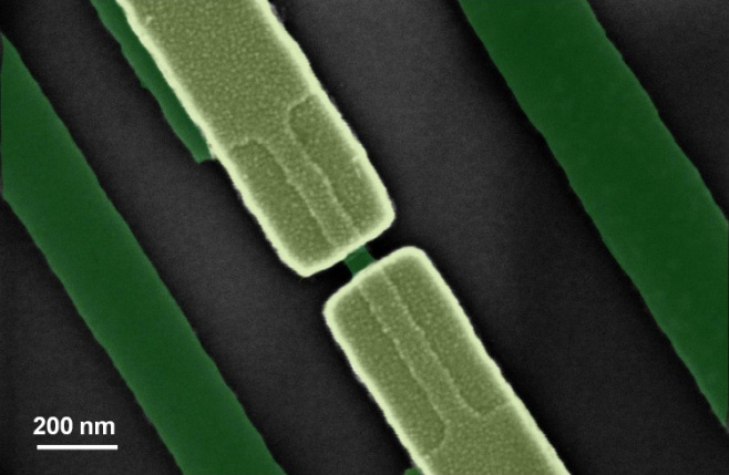
Figure 6.23: Colorized scanning electron microscope picture of one of the studied devices. The source and drain contacts are shown in yellow, below them is the structured MoS layer, shown in green. Originally published in [BSJ6](supporting material)
For the present investigation, around 30 devices have been manufactured by our research partner at Purdue university using an exfoliation method. For this, MoS (SPI Supplies) flakes have first been exfoliated onto SiO substrates using an established scotch tape technique. The used substrates are highly doped Si substrates with 20 nm SiO on top. The flakes have then been structured by e-beam lithography and successive plasma dry etching. Etching has been performed using 10 sccm of SF and Ar at a pressure of 3 Pa. Both the RF source and bias power have been set to
  and the etching time was 17 s. After this, 65 nm of Ni has been deposited and structured on top to form the source and drain contacts. A SEM image of one of these devices is shown in Figure 6.23. The devices’ gate areas are approximately 65
 50 nm. This is small enough to enable single defect characterization for this novel technology.
The thickness of the channel material among the available test chips has ranged from 5 nm to 15 nm. This reduces the band gap from 2.6 eV (direct) for single layer material to around 1.29 eV (indirect) for bulk material. The conduction state of the devices has been electrically controlled using the highly doped back gate. A schematic drawing of the devices is shown in Figure 6.24a. The basic characteristics of the devices—recorded in steps of −0.2 V with an integration time of 640 µs—are shown in Figure 6.24b-c.

Figure 6.24: (a) Schematics of the devices used during measurement. Few layers of MoS are located on top of a SiO wafer. Source and drain have been contacted on top, while the channel has been controlled using the back gate. (b) Transfer characteristics  (
( ) of an exemplary device with the subthreshold slope of
  . (c) Output characteristics () for the same device. These devices show normally-on characteristics. Originally published in [BSJ6]
The choice of gate stack and unintentional doping of the channel leads to the devices behaving as normally-on Schottky barrier (SB)-MOSFETs. The pinning of the Fermi level at the Ni-contacts close to the conduction band results
in the apparent high electron injection [150, 151]. As can be seen from the figure, the
subthreshold slope is around 1.1 V/dec and the on-off ratio is around  . The low subthreshold slope and on-off ratio are due to interface trap densities on the order of
  cm−2 and the Schottky barrier operation of the devices. The relatively linear output characteristics are a consequence of the small body thickness of the devices, and not a consequence of “ohmic”
contact behavior [151].
cm−2 and the Schottky barrier operation of the devices. The relatively linear output characteristics are a consequence of the small body thickness of the devices, and not a consequence of “ohmic”
contact behavior [151].
For the measurements, the devices have been kept in vacuum at  to 10−5 Torr and are also shielded from light. At each temperature, an initial () has been recorded to allow mapping of the drain current to
  . Subsequently, RTN traces have been recorded at a number of gate voltages. Once a defect suitable for extraction had been found, additional measurements have been performed in the voltage range where the defect
could be seen. Depending on the average charge transition times of the defect and the available measurement ranges, the device temperature has then been changed to characterize the thermal activation energy of the defect. A
number of defects have been characterized using this approach, four of which will be discussed here (henceforth called defects A-D).
. Subsequently, RTN traces have been recorded at a number of gate voltages. Once a defect suitable for extraction had been found, additional measurements have been performed in the voltage range where the defect
could be seen. Depending on the average charge transition times of the defect and the available measurement ranges, the device temperature has then been changed to characterize the thermal activation energy of the defect. A
number of defects have been characterized using this approach, four of which will be discussed here (henceforth called defects A-D).

Figure 6.25: Impact of single defects on different device characteristics: (a) Steps in the drain current of a transistor during () sweeps, equivalent to around 300 mV in . In large area devices many such defects would be visible as hysteresis, leading to a similar width of the hysteresis, but the individual contributions would not be observable. (b) A defect causing RTN. The
stochastic behavior of the defect causes a large variety of charge capture and emission times. (c) Similar to (b), but this defect shows a significant gate bias dependence. (d) A defect showing aRTN, periods
of noise are separated by periods of inactivity. The Markov chains necessary to model the respective defect’s behavior are shown in the insets (b) and (d). aRTN can not be described using a two state model and, in
this case, needs an additional neutral state. Originally published in [BSJ6]
Figure 6.25 shows a number of exemplary measurements recorded on these MoS devices. Figure 6.25a shows () measurements on device D, which has a defect with a relatively large impact introducing a hysteresis-like behavior. Figure 6.25b-c show RTN traces recorded on devices C and D to illustrate the bias dependence of the corresponding defects. It can be seen that
defect C is hardly affected by the gate bias, with its average capture and emission times staying relatively constant. For defect D on the other hand, the ratio between the average capture and emission times changes drastically with
gate bias. Both trapping behaviors of the defects may be modeled with a two-state model as shown in the inset of Figure 6.25b. A special
case is shown in Figure 6.25d, where defect B exhibits anomalous RTN behavior [22]. This defect shows phases of RTN interrupted by phases of inactivity where the defect dwells in its neutral state. The modeling of such charge trapping behavior
requires at least three defect states, as shown in the inset.
Once the data had been recorded, the approach based on hidden Markov models, as outlined in Section 5.1.3, has been
used to obtain the capture and emission times of the defects. The reason the author has chosen this approach for this study is due to both the comparatively high noise level of the measurement signal and the multi-state defect B.
The results are presented in Figure 6.26. Three of the defects—A, C, and D—show two-state RTN behavior, where at any voltage each
charge state can be associated with one characteristic time constant. Defect B, on the other hand, shows aRTN, which requires four transition rates to model, as shown in the inset of Figure 6.25d. The traps A and D show a bias dependence of the charge transition times as has been observed for oxide defects found in regular
Si/SiO devices. With increasing bias, their capture time decreases and their emission time increases. Defects B and C exhibit an unusual behavior due to the fact that their capture and emission times stay essentially constant over
the entire bias range where they could be characterized. A possible explanation for this is that they are located at a position where their trap level is not affected by the oxide field, i.e. in or on top of the channel. It is important to
recall at this point that the devices have been controlled by a backgate contact. For defect D, one can see that the capture time behavior hardly changes with temperature, unlike the emission time. This is an indication that the
energy barrier for charge capture is much lower than that for emission.

Figure 6.26: Capture and emission times extracted for four defects (symbols) and fits (lines). The charge transition times of defects A and D show a significant dependence on the gate bias, while the charge transition times of defects B and C seem to be unaffected by the gate bias. Defect B, which shows aRTN, is described using two sets of transition times due to its additional meta-stable state. The fits for defects B to D are from numerical simulation, while the fit for defect A is a linear fit. This is due to the current inability to simulate these devices at the low temperature at which defect A was measured. Originally published in [BSJ6]
From the charge transition times, the spatial and energetic positions of the defects could be estimated using electrostatic considerations as outlined in Section 5.1.4.
To validate the assumptions about the defect behavior in these backgated structures, TCAD simulations have been performed to mimic the charge trapping behavior of the defects. To assess which model to use for the defect simulations, the commonly used SRH and NMP defect models have been compared. For this, simulations have been performed for defects positioned above and below the channel using both the SRH and NMP defect models (see Figure 6.27a). The simulated defects have been positioned at a distance of 2 nm from the channel, at an energy close to the conduction band. The results of these simulations are shown in Figure 6.27b.

Figure 6.27: The SRH and NMP defect models both widely used for the description of interface and oxide defects. (a) The mechanisms for charge transfer as outlined in Section 3.1. (b) Simulations of the capture and emission times of defects placed at a distance of 2 nm above and below the channel. It can be seen that due to the lack of a backward energy barrier the SRH model, only one of the charge transition times features a meaningful temperature and bias dependence at any voltage. The SRH model can not describe the strongly voltage depen- dent capture and emission times as observed for defects A and D. For defect C the temperature dependence of both capture and emission time can not be described by the simple SRH model. Finally, multi state defects such as defect B can not be described at all using the simple SRH model, as it is limited to a defect with only a charged and a neutral state. Originally published in [BSJ6]
From the SRH model below the channel, the symptomatic behavior of this model can be seen. Depending on whether the effective energy of the defect is below or above the Fermi level of the channel, either the capture or emission time will be essentially constant. This is due to the fact that the model does not incorporate a backward barrier—the transition rate for this charge transfer is given by the carrier densities and the effective capture cross section. The same defect modeled using the NMP model yields continuously varying capture and emission times over the whole bias range, in agreement with the results obtained for defects A and D.
For defects simulated on atop the channel the bias dependencies for both defects look similar. The only bias dependence visible is due to the change of carrier density in the channel. The temperature behavior, however, does show a difference. Due to the missing backward barrier in the SRH model, one of the time constants—depending on the energetic position of the defect—will be independent of temperature. This rules out SRH behavior for defect C, where both charge transition times vary with temperature. Finally, defect B could only be characterized at one temperature due to the device failing at the first temperature change. Thus, its data do not allow to distinguish whether this defect follows SRH or NMP behavior.
Based on the observed behavior of the defects, simulations have been set up where the defects A and D are placed below the channel and the defects B and C above the channel. The defect parameters have then been optimized to match the extracted time constants, as seen in Figure 6.26.
The results of both the estimation equations and the numerical simulations are shown in Table 6.1. As can be seen from the table, no TCAD results could be obtained for defect A. This is due to the low temperatures (100 K and 120 K) of these measurements, which have led to convergence problems in the simulation.
Table 6.1: Extracted trap parameters, calculated with the analytical expressions Equations (5.33) and (5.36) (left), and from TCAD device simulation (right). Energies are relative to the conduction band edge. Originally published in [BSJ6]
| Type | Approximation | Fit Parameter | |||||||
| Defect | E |
z |
E a a |
 a a |
E |
R |
S |
z |
|
| 16 (A)b | 0.003 eV | −0.8 nm | — | — | — | — | — | — | |
| 25 (B) |  0.010 eV 0.010 eV |
≈8.0 nm | −0.149 eV | 0.99 eV | −0.017 eV | 0.80 | 1.60 | 8.5 nm | |
| 26 (C) | −0.018 eV |
≈8.0 nm | — | — | −0.016 eV | 0.69 | 1.38 | 8.0 nm | |
| 28 (D) | −0.843 eV | −3.2 nm | — | — | −0.640 eV | 0.52 | 0.33 | −1.7 nm | |
| a Parameters for three-state defects only b No TCAD fit | |||||||||
A graphical representation of the results is given in Figure 6.28.

Figure 6.28: Extracted spatial and energetic positions for defects A-D shown in a band diagram simulated for a device considering a 6 nm thin MoS layer. Defects A and D are located below the channel, while defects B and C are on top of it. The gate bias used for simulation was 1.2 V (opaque) and −4.2 V (semi-opaque). The charge transition times for
defects A and D change with the gate voltage as their position relative to the Fermi level shifts. The gray lines depict defect bands extracted for SiO [BSC6]. Originally published in [BSJ6]
From the characterization it follows that defects A and D reside at some distance (0.8 nm and 3.2 nm) below the channel in the SiO , and the defects B and C are in direct proximity to the MoS
 above the channel. Possible candidates for defects B and C thus include adsorbed water molecules or processing contaminants. Adsorbed water molecules in particular have already been linked to hysteresis behavior in
large area transistors [149] and adsorbates were visible on the wafer at the temperatures defect C was measured at. The more complex behavior of defect B,
however, could be caused by a more complex type of defect, e.g. an etching related defect. The fast charge transition times in the millisecond range at 100 K for defect A hint at an interface defect, while the behavior of
defect D, which is similar to defects measured in regular Si channel transistors, suggests a defect in the oxide. Compared to the estimations, the simulations place defect D closer to the interface, which is likely a result of the
approximations made in the estimation equations.
above the channel. Possible candidates for defects B and C thus include adsorbed water molecules or processing contaminants. Adsorbed water molecules in particular have already been linked to hysteresis behavior in
large area transistors [149] and adsorbates were visible on the wafer at the temperatures defect C was measured at. The more complex behavior of defect B,
however, could be caused by a more complex type of defect, e.g. an etching related defect. The fast charge transition times in the millisecond range at 100 K for defect A hint at an interface defect, while the behavior of
defect D, which is similar to defects measured in regular Si channel transistors, suggests a defect in the oxide. Compared to the estimations, the simulations place defect D closer to the interface, which is likely a result of the
approximations made in the estimation equations.
By measuring the responses of single defects in MoS channel transistors, we have been able to extract their characteristic charge capture and emission times in dependence on the gate bias. We have found that part of the defects are affected by the gate bias while others are
not. This is most likely due to the positions of the defects in the gate stack. By comparing the SRH and NMP trapping models to the behavior of the defects we have found that the SRH model is not sufficient to replicate their
behavior, and thus the NMP model has to be used for simulation—as in silicon channel devices. Using TCAD simulation we have been able to extract physical parameters of the defects, which provides us with some idea as to the
physical nature of each defect.

