« PreviousUpNext »Contents
Previous: 5.3 The Three Phases of the Electromigration Induced Vacancy Accumulation Top: 5 Results and Discussion Next: 5.5 Void Growth and Evolution
5.4 Electromigration Induced Stress at the Interfaces of Open TSVs
As described in Section 1.5 the open TSV technology is based on a hollow cylinder of overlapping conducting metal layers reaching from one side of the die to the other (cf. Figure 5.4). For FEM based simulation these arrangements with metal layer thick-
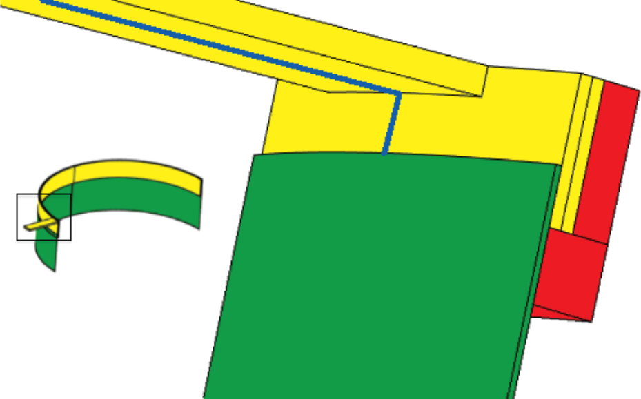
Figure 5.16.: Segment of the TSV closest to the current introducing planar interconnect line. The inset shows the half of the upper open TSV structures aluminium cylinder at the top and tungsten cylinder at the bottom. The blue line indicates the cross section for which the following simulation results are plotted. In this zone the highest current densities are foreseen and therefore EM has the biggest influence.
nesses in the order of tenth of a micrometer and the TSV diameter in the range of hundreds of micrometers make the meshing for 3D computations close to impossible. Therefore, a representative small segment of the open TSV has to be chosen in order to carry out simulations. This segment is located centrally under the planar interconnection which connects the open TSV with the integrated circuit, as shown in Figure 5.16. There the aspect ratio of the layer thicknesses and the overall structure is in the range of one to hundred, leading to an acceptable meshing quality inside the metal layers. Furthermore, as the results of Section 5.2 show, that a blocking interface has the highest impact on the vacancy pile-up and the high resistance of tungsten against EM, due to its low diffusion coefficient compared to aluminium, the vacancy flux calculations were restricted to the aluminium based structures.
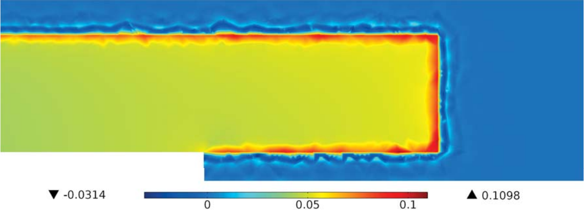
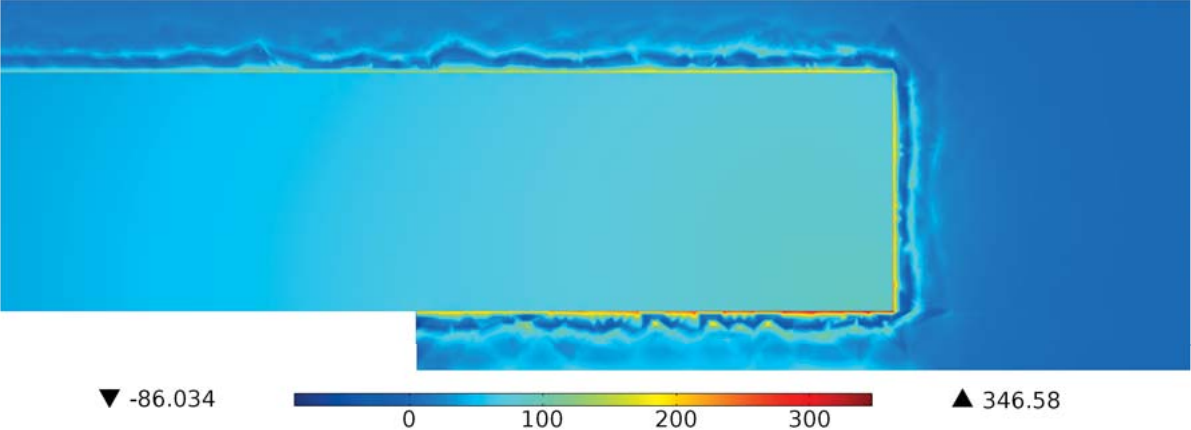
Figure 5.17 shows the appearance of the current crowding effect, as described in Section 5.1. This current crowding influences especially the vacancy pile-up for short times, as the highest vacancy concentration in the structure is
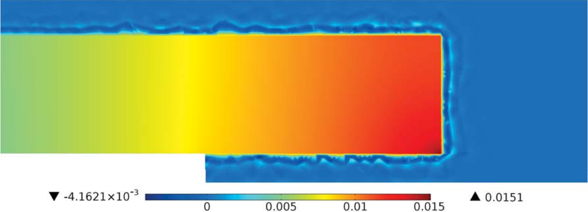
found at the corner for a simulated time period in the range of one second shown in Figure 5.  . In the phase of quasi-equilibrium, where the maximum vacancy
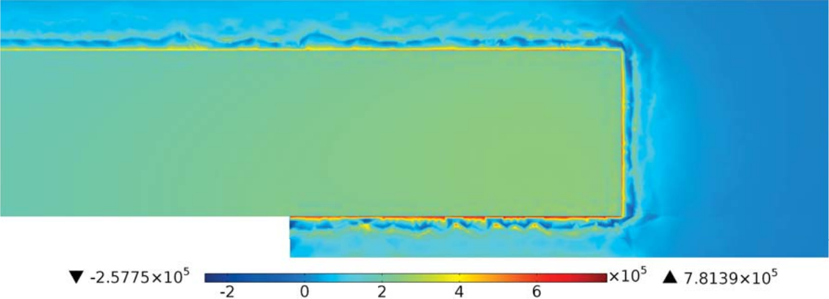
concentration stays constant, the vacancies pile-up in the whole structure due to the concentration gradient and stress gradient induced fluxes till the third phase starts. The vacancy concentration in this second phase is depicted in
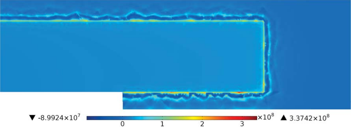
Figure 5.18b and shows that the vacancies are not transported to the interface but accumulated already before. In the third picture (Figure 5.18c) the vacancy concentration has very high values at the
tungsten/aluminium interface, but also
. In the phase of quasi-equilibrium, where the maximum vacancy
concentration stays constant, the vacancies pile-up in the whole structure due to the concentration gradient and stress gradient induced fluxes till the third phase starts. The vacancy concentration in this second phase is depicted in
Figure 5.18b and shows that the vacancies are not transported to the interface but accumulated already before. In the third picture (Figure 5.18c) the vacancy concentration has very high values at the
tungsten/aluminium interface, but also
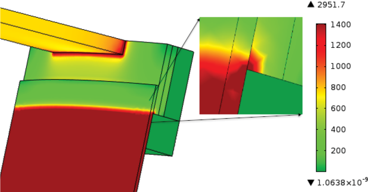
Figure 5.17.: Current density in  in the
simulated segment of the open TSV. At the bottom of the aluminium cylinder the current crowding is pronounced.
in the
simulated segment of the open TSV. At the bottom of the aluminium cylinder the current crowding is pronounced.
at the silicon oxide/aluminium interfaces. This behavior will get clear by considering the Von Mises stress distribution inside the open TSV shown in Figure 5.19.
For short times the stress is mainly driven by the shift of vacancies. Therefore, the highest stress, as shown in Figure 5.19a, is located in those areas where the highest vacancy concentrations are found (c.f. Figure 5.18a) with a linear dependence between them. As soon as phase two starts the stress increases over time and spreads out into the areas further away from the interface shown in Figure 5.19b according to the behavior described in Section 5.3. The vacancy concentration stays constant at the interface and the concentration in the rest of the aluminium rises asymptotically to the one of the interface. After this second phase the stress reaches a value where the vacancy concentration diverges. Due to the tendency of the aluminium to shrink, while the surrounding material tends to stay in size, a high stress is built up at the interfaces (cf. Figure 5.19c) leading in the real structure to cracking or the formation of voids. At this point the simulation can be interrupted as a so called soft failure has been reached [35].
The development of the maximum Von Mises stress in the structure versus time is shown in Figure 5.20. By choosing a stress threshold for cracking or void formation according to Section 3.5 for every current density a TTF can
be found and fitted to Black’s equation. In Figure 5.21 the data points for a threshold Von Mises stress of  are
shown. Furthermore, the graph of a fit to Black’s equation is shown. Due to the chosen logarithmic scale of the axis the fitted graph is represented by a straight line. The fitted exponent of the current density in (2.6) was found to be
0.74.
are
shown. Furthermore, the graph of a fit to Black’s equation is shown. Due to the chosen logarithmic scale of the axis the fitted graph is represented by a straight line. The fitted exponent of the current density in (2.6) was found to be
0.74.
(a) 
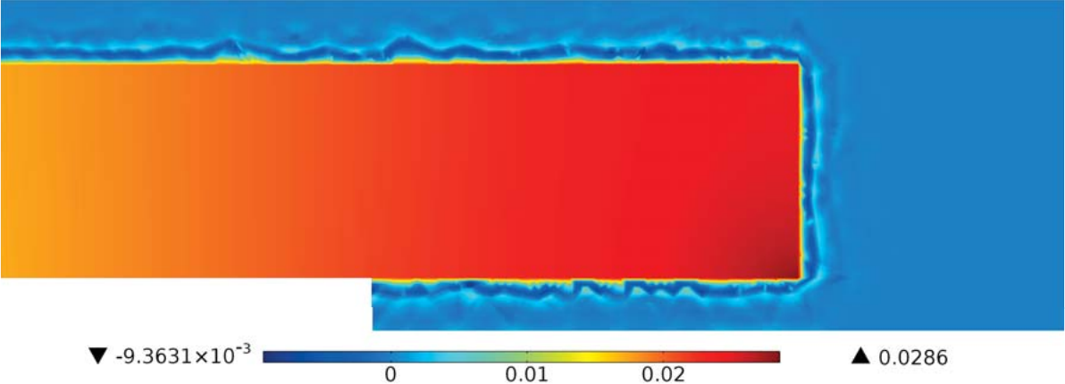
(b) 
(c) 
Figure 5.18.: Relative vacancy concentration deviation  piled up in the structure for three different simulated time periods. The cross section is the cut of the blue line in Figure 5.16.
(a)
(b)
(c)
Figure 5.19.: Von Mises stress in  build-up in the structure
for three different simulated time periods. The cross section is the cut of the blue line in Figure 5.16.
build-up in the structure
for three different simulated time periods. The cross section is the cut of the blue line in Figure 5.16.
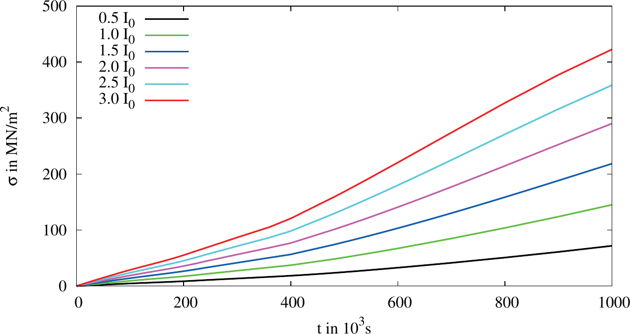
Figure 5.20.: Maximum Von Mises stress build-up at the interface for different currents.
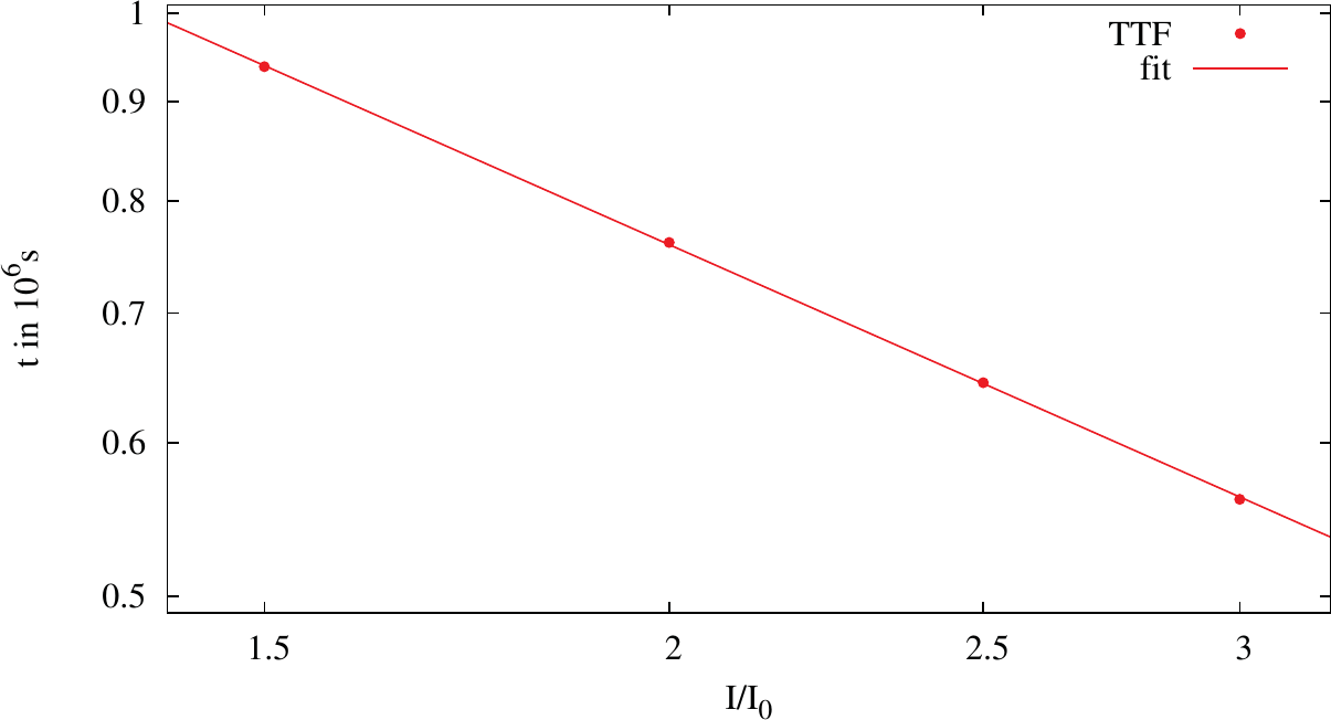
Figure 5.21.: TTF for different currents with a fitting to Black’s equation. The axis are logarithmically scaled.
Previous: 5.3 The Three Phases of the Electromigration Induced Vacancy Accumulation Top: 5 Results and Discussion Next: 5.5 Void Growth and Evolution