« PreviousUpNext »Contents
Previous: 1.3 Copper Based Interconnect Fabrication Top: 1 Introduction Next: 1.5 Open TSV Structure
1.4 Three-Dimensional Integration
Commonly ICs are built in a planar 2D design style. For miniaturization and performance increase of electronic systems the increased utilization of 3D integration methods is unavoidable [1]. Thereby dies are stacked and have to
get vertically connected to enable the signal flow between them. Therefore novel interconnect structures are introduced reaching through the single dies and connecting from one die to the other. This increases besides the area
efficiency (for  dies in a
  package in the range of 50%) also the volumetric
efficiency which is nowadays only in the range of 0.01% and potentially allows shorter interconnections than in 2D configurations enabling higher operation speed and lower power consumption. On one side this is of particular
importance for high performance computing as in synchronous operating mode the latency of the clock signals depending on the interconnection length is a limiting factor [7]. On the
package in the range of 50%) also the volumetric
efficiency which is nowadays only in the range of 0.01% and potentially allows shorter interconnections than in 2D configurations enabling higher operation speed and lower power consumption. On one side this is of particular
importance for high performance computing as in synchronous operating mode the latency of the clock signals depending on the interconnection length is a limiting factor [7]. On the
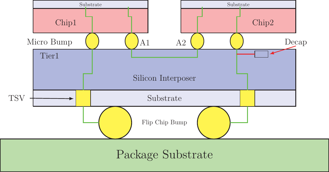
Figure 1.3.: Schematic of a chip-to-wafer bonded structure. Stapled dies hold together by solder bumps.
other side 3D integration also allows the stapling of dies based on different technologies, which is called heterogeneous integration (e.g. analog, digital, sensors, antennas, and power electronics) and different technology nodes [71].
Bonding is the process of mounting one wafer or die onto another. The first method is termed wafer bonding. Thereby two wafers are bonded before the wafers are cut into single dies. Due to the easier alignment this method was
developed first. The second possibility is called chip-to-wafer bonding. With this method the dies can have different dimensions giving more flexibility as one chip can carry more then an other chip.
Figure 1.3 shows a possible combination of different dies connected by solder bumps in the chip-to-wafer configuration [108].
The available bonding processes can be divided into two kinds. The first is called direct bonding, where no intermediate layer is separating them. This type is separable into molecular bonding and anodic bonding. The second is the bonding with intermediate layers, where polymer, glass [79] or solder bumps are put in between them to hold the wafers together [140]. In the next section TSV structures are introduced with a special focus on the direct bonding method, based on a device presented by Kraft et al. [83].
« PreviousUpNext »ContentsPrevious: 1.3 Copper Based Interconnect Fabrication Top: 1 Introduction Next: 1.5 Open TSV Structure