« PreviousUpNext »Contents
Previous: 4.5 Summary Top: Home Next: Bibliography
5 Conclusions & Outlook
In the present thesis, the behavior of state-of-the-art 4H-SiC MOSFETs under temperature and voltage stress was assessed with a focus on the impact on the reliability under use-conditions. Numerous devices from multiple manufacturers were characterized using electrical measurements and compared regarding their bias temperature instability. A major achievement in this work was the identification of two independent dominant components which contribute do BTI on 4H-SiC based devices and result in the observed characteristics.
The first component, which is especially visible as a gate voltage hysteresis in the subthreshold regime of the transfer characteristics, originates from hole capture in trap states at the 4H-SiC/SiO2 interface. Unlike the
second component, these states are fully discharged in normal device operation (e.g. AC-use conditions) via an inversion gate pulse above the threshold voltage within nanoseconds. Furthermore, no impact on the long-term device
reliability was found even for several million charging/discharging cycles indicating a fully-reversible charging/discharging mechanism which does not cause any permanent damage to the SiC/SiO2 interface by creating
new interface defects. However, the magnitude of the observed voltage shift caused by the first component strongly depends on the crystal plane on which the inversion layer forms. This results in a one order of magnitude higher
interface state density for crystal planes which are parallel to the  -axis, which was observed on all available SiC-MOSFET by different manufacturers by
today. The atomic origin of the defect states, which are responsible for the first component, presumably are carbon dangling bonds on the SiC-side of the SiC/SiO2 interface.
-axis, which was observed on all available SiC-MOSFET by different manufacturers by
today. The atomic origin of the defect states, which are responsible for the first component, presumably are carbon dangling bonds on the SiC-side of the SiC/SiO2 interface.
The second shift component is similar to what is observed on silicon based devices and most likely originates from trap states spatially located at the SiO2-side of the SiC/SiO2 interface and energetically located close to the conduction band of 4H-SiC (border states). These states exhibit broadly distributed activation energies for capture and emission. It was demonstrated that all SiC-MOSFETs from different manufacturers available on the market show nearly identical voltage shift behavior even under a low-bias operation close to the threshold voltage. A preconditioned BTI measurement pattern tailored to SiC based devices was demonstrated, which allows for an independent determination of the second component. Furthermore, it was shown that the preconditioned measurement is robust with respect to delay- and readout- timing variations since fully-reversible intrinsics cancel out. Therefore, the preconditioned measurement technique allows for a more accurate lifetime prediction.
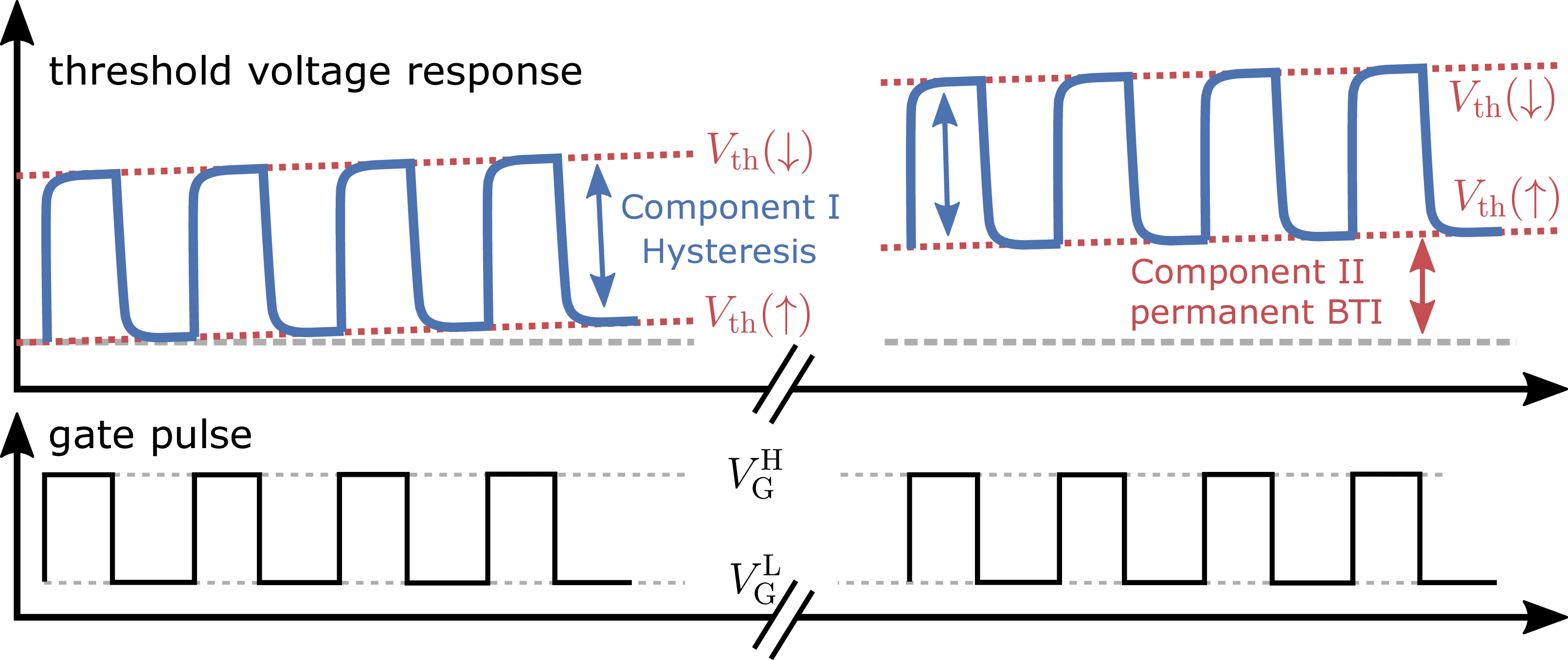


To summarize, both components contribute to the final threshold voltage behavior of the device. A sketch of the evolution of the threshold voltage during application is given in Fig. 5.1 with the gate signal (bottom) and the corresponding threshold voltage (top). Assuming the low level of the gate pulse is in accumulation during  , interface states (hysteresis, component I) are
continuously completely charged and discharge while switching from to
, interface states (hysteresis, component I) are
continuously completely charged and discharge while switching from to  , which results in the fully reversible hysteresis
effect (blue), meaning the threshold voltage for turn-on
, which results in the fully reversible hysteresis
effect (blue), meaning the threshold voltage for turn-on  will be
significantly lower than the threshold voltage for turn-off
will be
significantly lower than the threshold voltage for turn-off  . On the other
hand, border states are increasingly charged during long-term operation, which in the end leads to device degradation (e.g. a slight increase in the on-resistance), due to the increasing threshold voltage (permanent voltage shift,
red).
. On the other
hand, border states are increasingly charged during long-term operation, which in the end leads to device degradation (e.g. a slight increase in the on-resistance), due to the increasing threshold voltage (permanent voltage shift,
red).
As a final step, the impact of a high thermal budget on the charging state of the SiC/SiO2 interface was investigated throughout a series of multiple high temperature manufacturing processes. It was shown that such high temperature processing steps in combination with an electric field result in an accumulation of fixed positive charges at the SiC/SiO2 interface. The origin of these charges is still unknown. Possibly they originate from ions with low diffusion coefficients at room temperature or are related to hydrogen, which dissociates from precursor states at such high temperatures and is introduced during the deposition of the polycrystalline silicon gate contact. An energy barrier of approximately 1.3 eV was extracted from the experimental data, which is in good agreement with values proposed from theoretical hydrogen related degradation mechanism like the H-release model [48, 58, 132, 133].
Although considerable progress in the understanding of the aforementioned topics could be accomplished in this thesis, several question regarding charge trapping on SiC based devices remain:
-
• Functioning annealing techniques, which result in an significant decrease of the hysteresis, are still unknown. Although annealing in NO containing atmospheres results in an enormous increase in the electrical device performance, the hysteresis seems to be unaffected. Due to this, different gas compositions like ammonia (NH3) are intensively investigated and might result in a better passivation of the SiC/SiO2 interface.
-
• The origin and microscopic species of the positive charge accumulation during high temperature processing steps remains unknown. Instead of investigating complicated, real devices with complex surface morphology, which furthermore undergo hundreds of processing steps, a simpler approach might be more suited for subsequent research. Here a basic Si/SiO2/SiC MOS structure, which is stepwise subjected to an increasing thermal budget and measured afterwards, will allow for a much faster and cheaper examination of the topic.
« PreviousUpNext »Contents
Previous: 4.5 Summary Top: Home Next: Bibliography