« PreviousUpNext »Contents
Previous: 2.4 Time and temperature dependence Top: 2 On the first Component: the Subthreshold Hysteresis Next: 2.6 Charge pumping
2.5 Crystal face dependence
All results discussed above are extracted from in-house MOSFETs with the active channel on the a-face, (11 0)-plane. To obtain a complete picture, we also investigated MOSFETs
with the channel on the Si-face, (0001)-plane. For these devices, the same trend is observed, although
0)-plane. To obtain a complete picture, we also investigated MOSFETs
with the channel on the Si-face, (0001)-plane. For these devices, the same trend is observed, although  is in the range of millivolts and therefore not as
pronounced in the ID -VG curves (not shown). This is a surprising outcome if one considers the, in general, much lower mobility for devices with the active channel on the Si-face. Compared to their a-face counterparts, the typical
mobility of Si-face MOSFETs, which were subjected to an identical interface passivation, is 2 to 3 times lower. In our case, the extracted low-field mobility of the in-house Si-face devices is
is in the range of millivolts and therefore not as
pronounced in the ID -VG curves (not shown). This is a surprising outcome if one considers the, in general, much lower mobility for devices with the active channel on the Si-face. Compared to their a-face counterparts, the typical
mobility of Si-face MOSFETs, which were subjected to an identical interface passivation, is 2 to 3 times lower. In our case, the extracted low-field mobility of the in-house Si-face devices is  , whereas the a-face devices show a 3 times higher mobility of
  , which is consistent with recent studies [114].
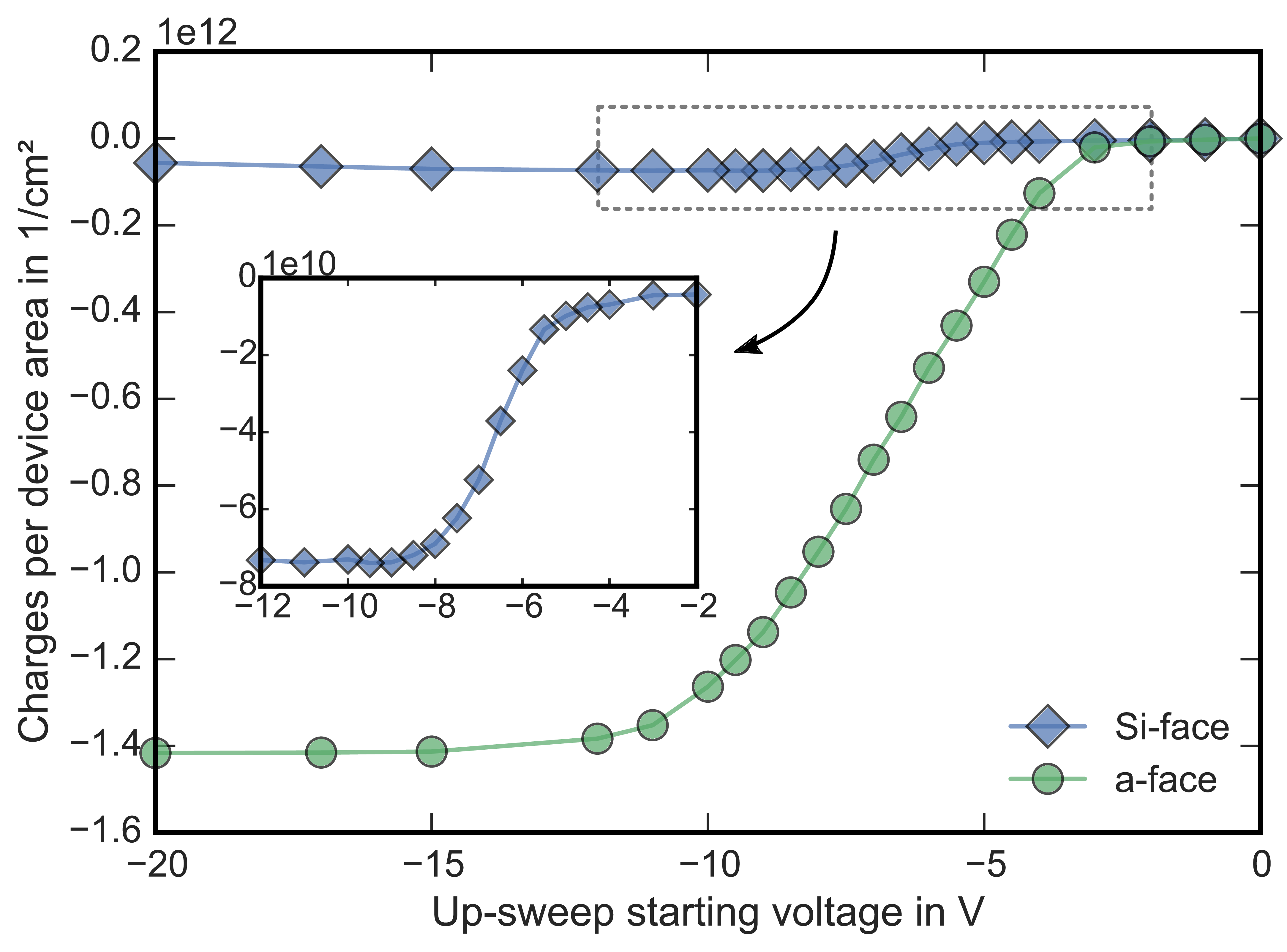
Figure 2.24: Trapped charges at the interface per device area as a function of the up-sweep starting voltage for a Si-face (diamonds, blue) and an a-face (circles, green) device. The same trend is observed on both crystal faces although the effect is more pronounced on the a-face. The inset provides a closer look on the Si-face curve.
From  , the number of trapped charges
  per device area
  , can be extracted using the the formula of the capacitance and is given by

with the relative permittivity of SiO2,  , the vacuum permittivity
 , the oxide thickness
  and the electronic charge
  . Fig. 2.24 shows extracted from via (2.12) for both crystal faces as a function of the up-sweep starting voltage. It is important that, despite the lower channel mobility, also the interface trap density
calculated from is about one order of magnitude lower on Si-face
(diamonds, blue) devices than on a-face (circles, green) MOSFETs. For both device designs, no permanent component is present in the hysteresis. Even after millions of charging-discharging cycles, which occur during AC-use
conditions, and therefore the hysteresis remains constant
[111].
. Fig. 2.24 shows extracted from via (2.12) for both crystal faces as a function of the up-sweep starting voltage. It is important that, despite the lower channel mobility, also the interface trap density
calculated from is about one order of magnitude lower on Si-face
(diamonds, blue) devices than on a-face (circles, green) MOSFETs. For both device designs, no permanent component is present in the hysteresis. Even after millions of charging-discharging cycles, which occur during AC-use
conditions, and therefore the hysteresis remains constant
[111].
To summarize the dependence of the subthreshold sweep hysteresis on the SiC crystal plane, both Si-face and a-face MOSFETs show the same trend. However, the total amount of trapped charges extracted from the ID -VG curves is smaller on the Si-face, which is in contrast to the lower mobility of these devices. An explanation for the discrepancy between a lower trap density and lower mobility is given in the next section.
« PreviousUpNext »ContentsPrevious: 2.4 Time and temperature dependence Top: 2 On the first Component: the Subthreshold Hysteresis Next: 2.6 Charge pumping