« PreviousUpNext »Contents
Previous: 2.7 Possible atomic origin Top: 2 On the first Component: the Subthreshold Hysteresis Next: 2.9 Relevance of the hysteresis on normal device operation
2.8 Hysteresis on devices by various manufacturers
To compare the hysteresis of 4H-SiC MOSFETs produced by different manufacturers, the transfer characteristics have been extracted from devices of the three most important manufacturers. The outcome is shown in Fig. 2.34 for the previous (left column) and current (right column) generation of devices. MOSFETs with a lateral channel design are shown in green, whereas devices with a trench channel design are indicated in blue. Devices are labeled A, B and C to maintain manufacturer anonymity.
Fig. 2.35 shows the number of trapped charges per device area extracted from the input characteristics in Fig. 2.34. The left bar always shows the previous technology generation of each manufacturer, whereas the right one shows the current device generation. As can be
immediately seen, the main impact on the sweep hysteresis originates from the crystal plane of the inversion channel (trench or lateral) and is nearly independent of the device manufacturer. For Si-face devices,  is in the range of
0.1 × 10¹²/cm2 to 0.2 × 10¹²/cm2, whereas for trench devices, is in the range of
0.9 × 10¹²/cm2 to 1.1 × 10¹²/cm2.
is in the range of
0.1 × 10¹²/cm2 to 0.2 × 10¹²/cm2, whereas for trench devices, is in the range of
0.9 × 10¹²/cm2 to 1.1 × 10¹²/cm2.
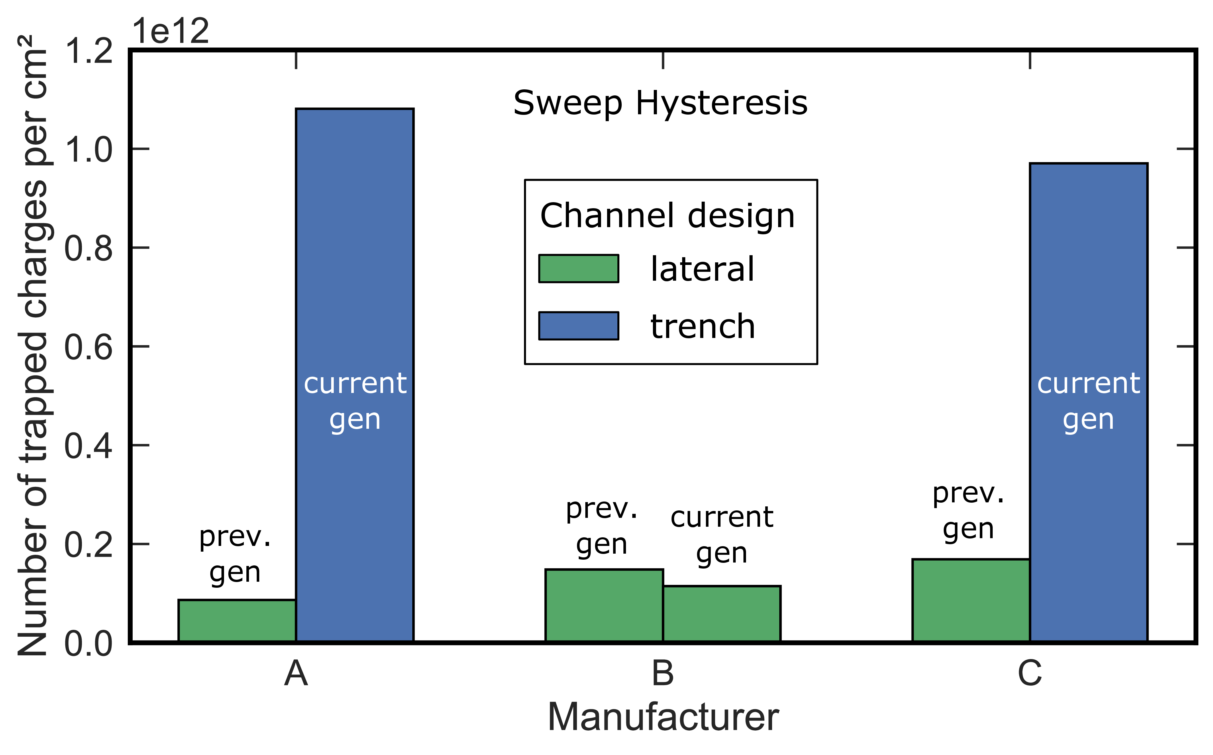
Figure 2.35: Number of trapped charges extracted from the input characteristics for three different manufacturers. The left bar corresponds to the previous generation of each manufacturer, whereas the right bar shows the per- formance of the current device generation. As can be seen, the main impact on the sweep hysteresis originates from the crystal plane of the channel and is nearly independent of the device manufacturer.
Previous: 2.7 Possible atomic origin Top: 2 On the first Component: the Subthreshold Hysteresis Next: 2.9 Relevance of the hysteresis on normal device operation