« PreviousUpNext »Contents
Previous: 3 On the second Component: Bias Temperature Instability Top: 3 On the second Component: Bias Temperature Instability Next: 3.3 Preconditioned BTI measurements
3.2 Similarities in BTI of commercially available SiC-power MOSFETs
Here, we compare the threshold voltage instability of commercially available, application ready SiC-MOSFETs under PBTS. The fact that SiC based MOSFETs show an increased bias temperature instability is well known from countless studies [25, 31, 33, 36–39, 42, 43, 106, 118, 122–127]. However, most of these studies are based on devices which are only optimized for single parameters like mobility or voltage shift characteristics and therefore not ready for application. An application ready device on the other hand, needs to be reliable, meaning every device parameter has to stay within a well defined threshold within the devices lifetime. Furthermore, these MOSFETs have to provide excellent electrical characteristics. Therefore, such a device needs to be optimized with respect to multiple parameters like channel mobility, oxide reliability, and bias temperature instability. Due to this, compromises (trade-offs) are inevitable for certain key-parameters. This results in the fact that commercially available devices usually will not perform as well as devices reported in literature, where (in general) test structures optimized for a single parameter are investigated.
Therefore, this section provides an overview on the BTI of state-of-the-at SiC-MOSFETs, which are already available on the market and optimized for power-electronics and reliability. It will be shown that all of these devices show very similar drift characteristics in the low-bias regime.
3.2.1 Low-field mobility
At first I start by analyzing the low-field channel mobility  of the devices, which is usually a good indicator
for the quality of the SiC/SiO2 interface. The mobility was extracted via the input characteristics using the method of Ghibaudo [78] (c.f Section 1.3.3) for the devices from
manufacturers A, B, and D. Manufacturer C is missing due to unknown channel dimensions of the device. The extracted mobility values are 8 cm2/(V s) for device A,
19 cm2/(V s) for device B and 58 cm2/(V s) for device D. These mobility values are far below the bulk mobility of 4H-SiC, which is around
800 cm2/(V s) [6] and furthermore below the maximum reported mobilities achieved in some recent studies (e.g. up to 100 cm2/(V s) in Ref. [110, 114]). Note that
most of these studies are based on lateral MOSFETs, which are not optimized for power electronics and reliability. Therefore, a lower mobility is expected for commercially available SiC-MOSFETs which have to be reliable in high
power and high temperature use-conditions.
of the devices, which is usually a good indicator
for the quality of the SiC/SiO2 interface. The mobility was extracted via the input characteristics using the method of Ghibaudo [78] (c.f Section 1.3.3) for the devices from
manufacturers A, B, and D. Manufacturer C is missing due to unknown channel dimensions of the device. The extracted mobility values are 8 cm2/(V s) for device A,
19 cm2/(V s) for device B and 58 cm2/(V s) for device D. These mobility values are far below the bulk mobility of 4H-SiC, which is around
800 cm2/(V s) [6] and furthermore below the maximum reported mobilities achieved in some recent studies (e.g. up to 100 cm2/(V s) in Ref. [110, 114]). Note that
most of these studies are based on lateral MOSFETs, which are not optimized for power electronics and reliability. Therefore, a lower mobility is expected for commercially available SiC-MOSFETs which have to be reliable in high
power and high temperature use-conditions.
3.2.2 Measurement pattern
To investigate the threshold voltage instability of the devices under low-bias, all MOSFETs were subjected to positive bias stress according to the pattern sketched in Fig. 3.1.
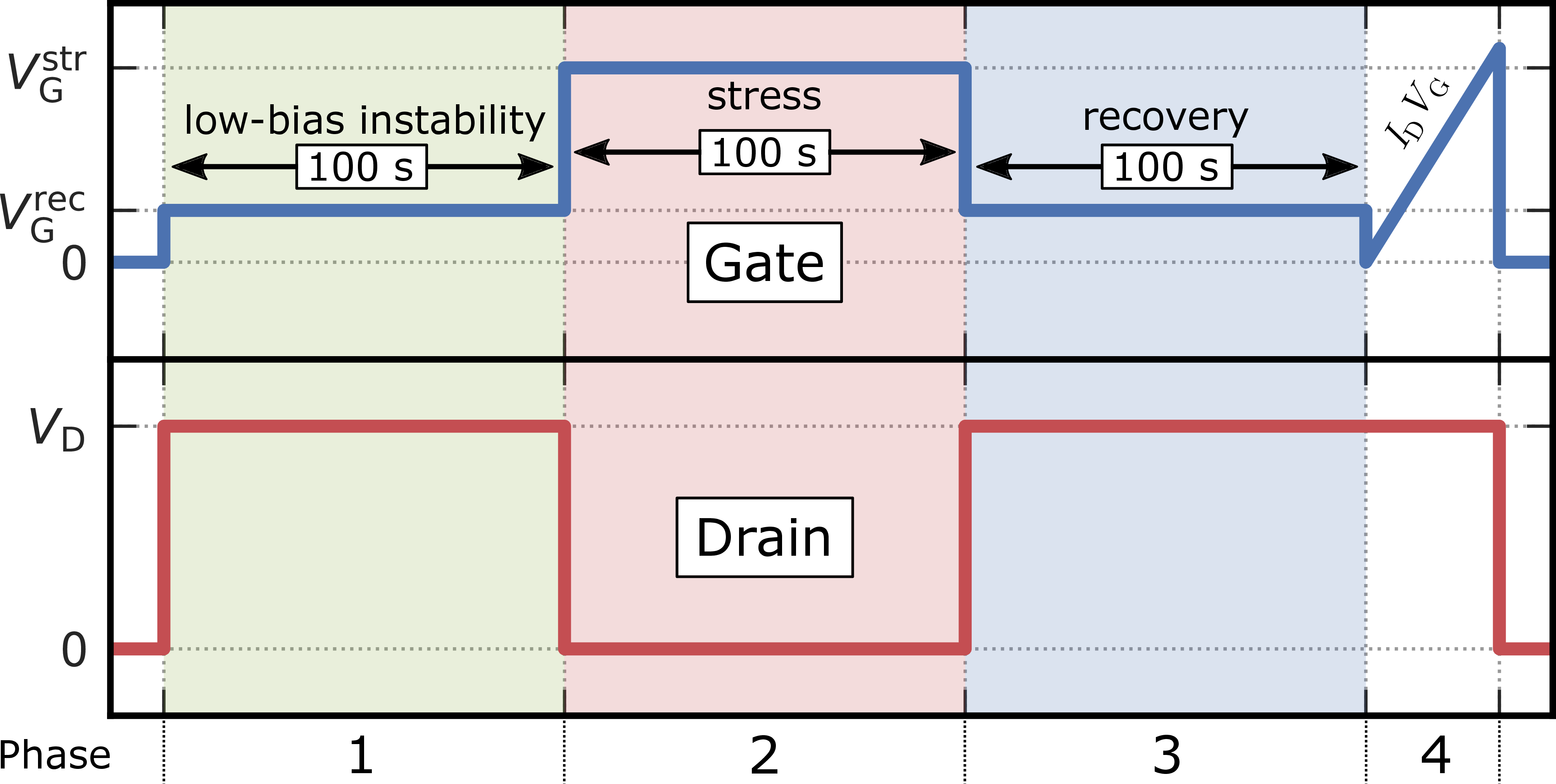
The measurement sequence consists of 4 different phases starting with a bias switch from  to
to  , which is close to the
data-sheet threshold voltage of all devices. Here, the bias is held for 100 s to measure the low-bias drain current instability (phase 1). Afterwards, a stress cycle is performed at a gate voltage of
, which is close to the
data-sheet threshold voltage of all devices. Here, the bias is held for 100 s to measure the low-bias drain current instability (phase 1). Afterwards, a stress cycle is performed at a gate voltage of  for a stress time of
 (phase 2). The stress
voltage was chosen so that the applied positive bias stress of 25 V is within the allowed maximum gate bias range mentioned in the data sheets of all devices. After the stress phase, another low-bias phase at is measured (phase 3) to
investigate the time dependent recovery of the threshold voltage shift
(phase 2). The stress
voltage was chosen so that the applied positive bias stress of 25 V is within the allowed maximum gate bias range mentioned in the data sheets of all devices. After the stress phase, another low-bias phase at is measured (phase 3) to
investigate the time dependent recovery of the threshold voltage shift  after the 25 V positive bias stress. At
the end of the measurement pattern (phase 4), an ID -VG curve from −2 V to 26 V is measured to be able to calculate from the change in the drain current during the
phases 1 and 3. The whole procedure was repeated at various temperatures between −60 °C and 150 °C on the same device to also investigate the temperature dependence of the low-bias instability and
recovery traces. The drain voltage was set to
after the 25 V positive bias stress. At
the end of the measurement pattern (phase 4), an ID -VG curve from −2 V to 26 V is measured to be able to calculate from the change in the drain current during the
phases 1 and 3. The whole procedure was repeated at various temperatures between −60 °C and 150 °C on the same device to also investigate the temperature dependence of the low-bias instability and
recovery traces. The drain voltage was set to  in the phases 1, 3,
and 4, whereas
in the phases 1, 3,
and 4, whereas  was set to 0 V during the stress (phase
2) to suppress self heating, hot carrier degradation and non-uniform electric oxide fields.
was set to 0 V during the stress (phase
2) to suppress self heating, hot carrier degradation and non-uniform electric oxide fields.

3.2.3 Low-bias instability
We start by analyzing the drain current  transients of the devices under low-bias
in phase 1. Here, the bias is switched from from
transients of the devices under low-bias
in phase 1. Here, the bias is switched from from  to , which is slightly above
the threshold voltage
to , which is slightly above
the threshold voltage  of all devices (3 V to 4 V).
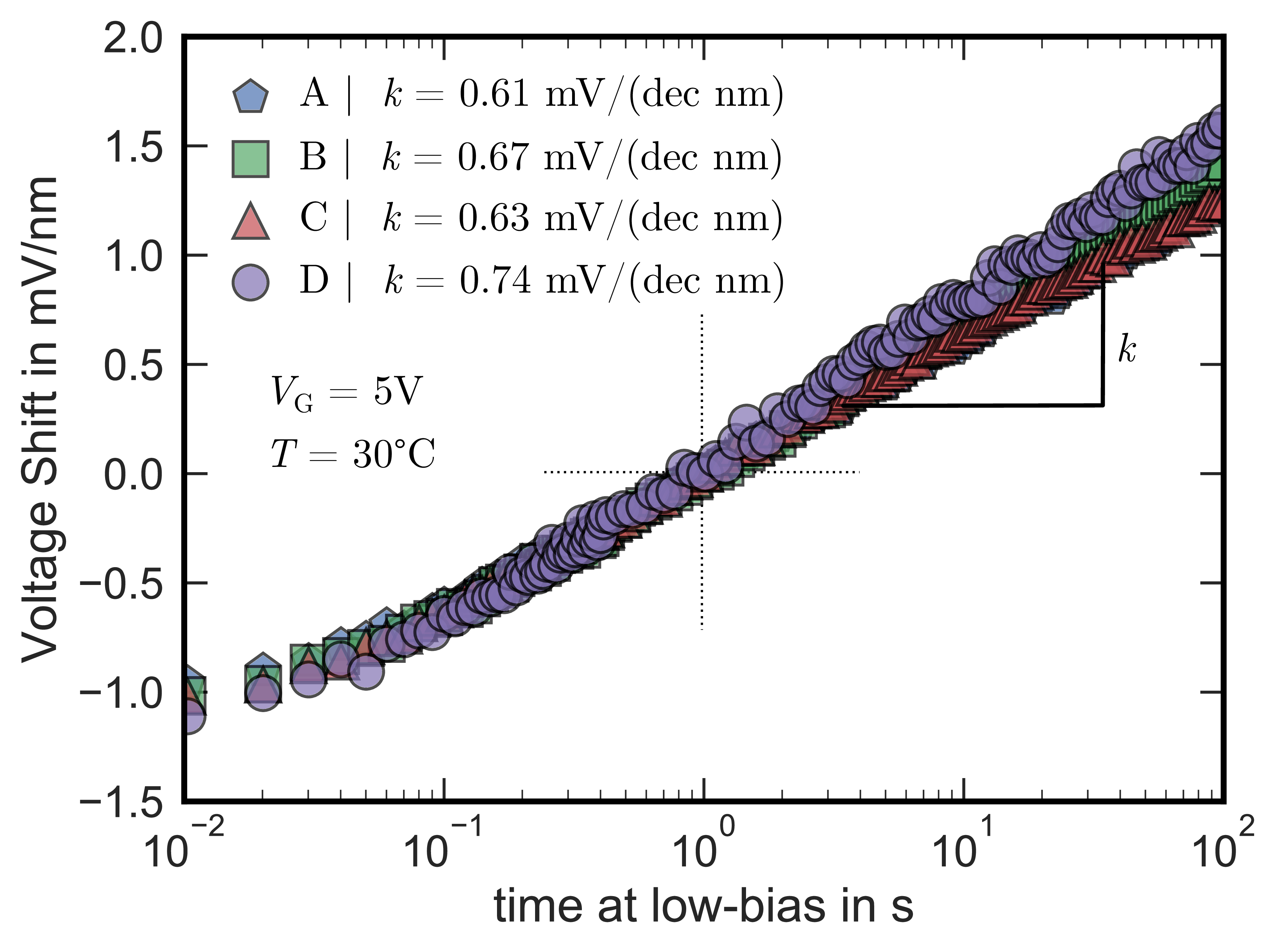
Even at such a low gate bias, drain current transients are observed for all devices. The resulting voltage shift is indicated in Fig. 3.2. All devices show similar drift behavior in the low gate bias regime at 30 °C within the measurement
window, which ranges from 10 ms to 100 s. follows a logarithmic behavior with slopes
around of 0.65 mV per decade per nanometer oxide thickness within our narrow experimental window. Here, is normalized to the oxide thickness
of all devices (3 V to 4 V).
Even at such a low gate bias, drain current transients are observed for all devices. The resulting voltage shift is indicated in Fig. 3.2. All devices show similar drift behavior in the low gate bias regime at 30 °C within the measurement
window, which ranges from 10 ms to 100 s. follows a logarithmic behavior with slopes
around of 0.65 mV per decade per nanometer oxide thickness within our narrow experimental window. Here, is normalized to the oxide thickness  to account for differences in between the various manufacturers.
Since the input characteristics used for the calculation of is shifted to the end of the measurement pattern,
the reference value of the threshold voltage of all tested devices originates from the amount of charges captured and emitted during the whole test procedure. Therefore, the real point of origin is unkown and all traces in Fig.
3.2 are vertically shifted to a threshold voltage shift of 0 V after 1 s (dotted cross)
for better comparability. The same holds for all subsequent figures in this section.
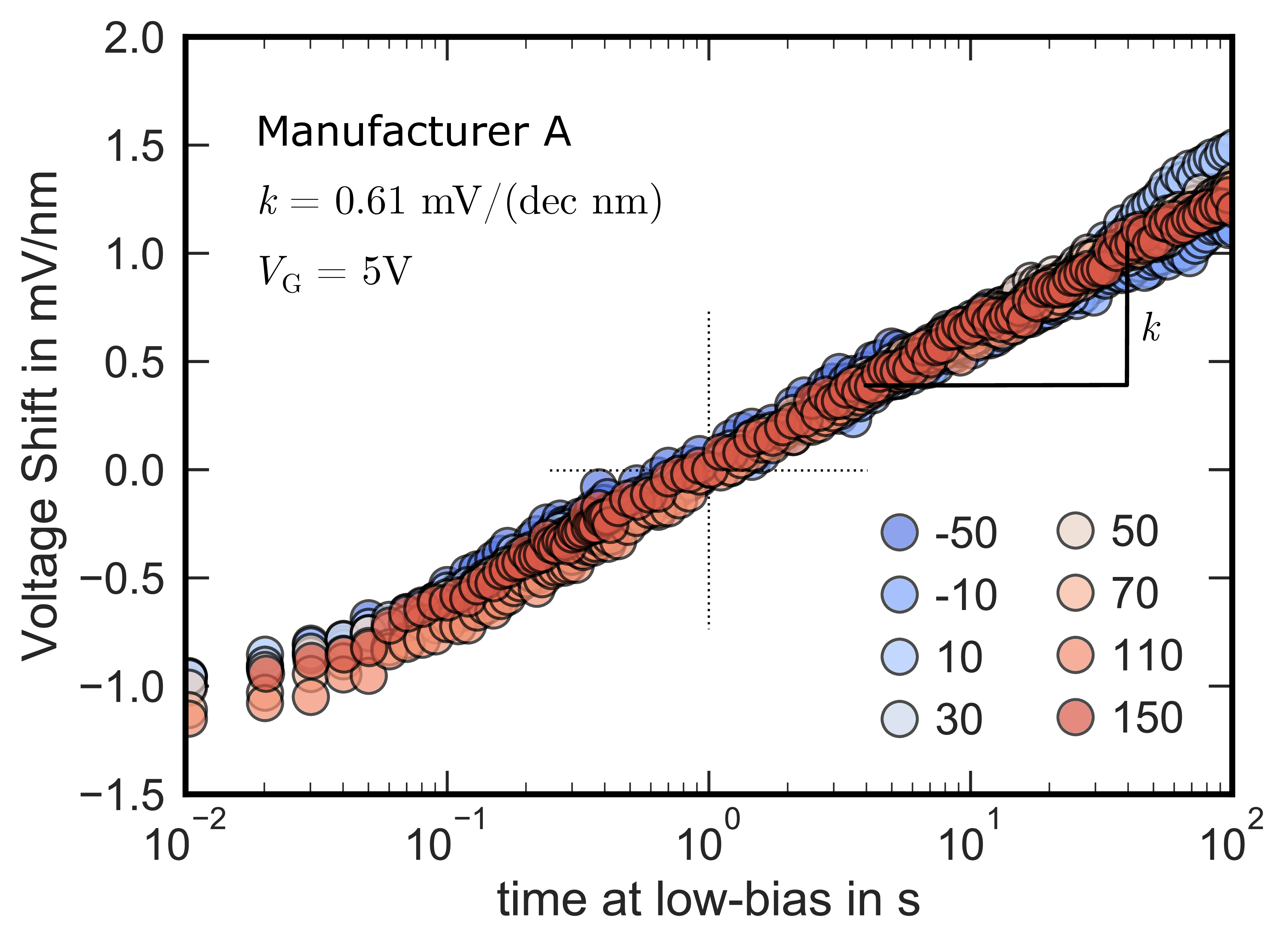
Figure 3.3: Temperature dependence of the low-bias voltage shift per nanometer oxide thickness. Within a temperature range from −50 °C to 150 °C no temperature dependence is visible, which indicates broadly distributed activation energies as described in Section 1.2.1. The picture shows the traces of device A. Devices B, C, and D show the same behavior.
Temperature dependence of the low-bias voltage shift
The temperature dependence of the low-bias threshold voltage instability of device A is shown in Fig. 3.3. Within
the measurement range between −50 °C and 150 °C the low-bias instability has a constant value of  , which is independent of the device temperature within the investigated temperature range. The same trend is observed for the devices B, C, and D (not shown). Such a temperature independent
low-bias is most likely observed due to broadly
distributed activation energies within the, in this special case, narrow experimental window (c.f Section 1.2.1).
, which is independent of the device temperature within the investigated temperature range. The same trend is observed for the devices B, C, and D (not shown). Such a temperature independent
low-bias is most likely observed due to broadly
distributed activation energies within the, in this special case, narrow experimental window (c.f Section 1.2.1).
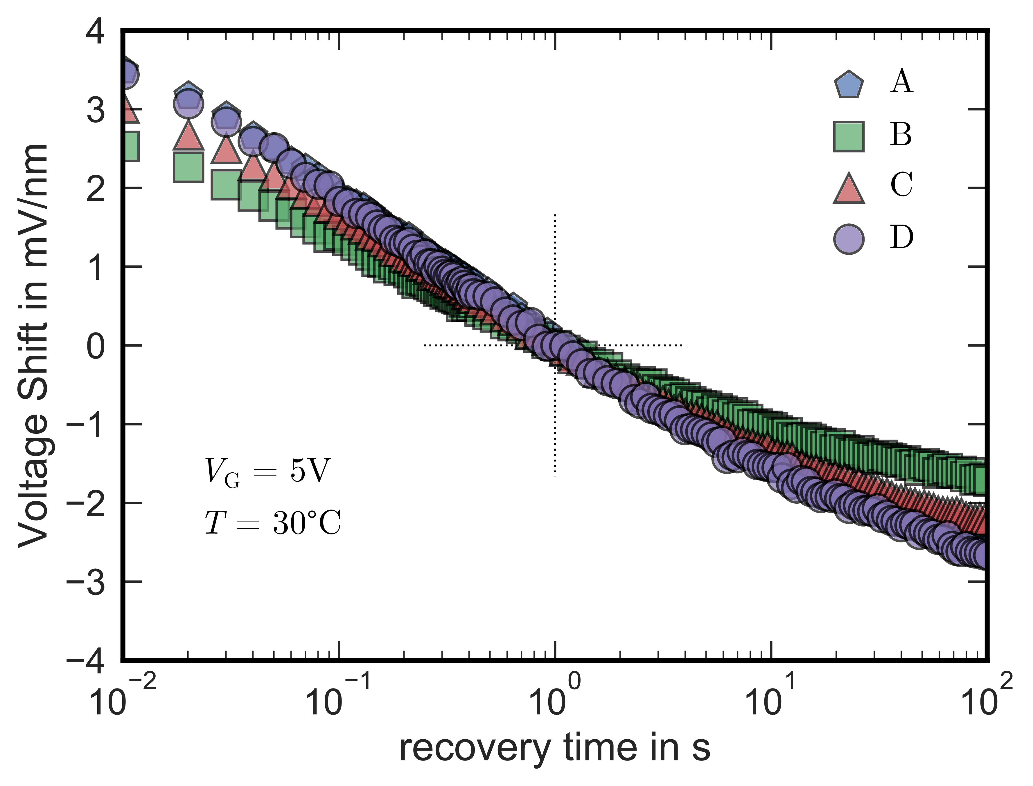
3.2.4 Recovery after high bias stress
The recovery traces of at  after the 100 s long 25 V
stress at 30 °C are shown in Fig. 3.4. Again, we observe a similar behavior for devices A (-1.5
mV/dec/nm), B (-1.1 mV/dec/nm), C (-1.4 mV/dec/nm) and D (-1.5 mV/dec/nm). The temperature dependence of the recovery traces for device A is shown in Fig. 3.5. Devices B, C and D show a similar behavior (not shown). Unlike the low-bias instability, the recovery slope
increases with decreasing temperature and furthermore deviate from the power-law behavior observed withing the narrow experimental window during phase 1. Cold temperatures slow down the emission of trapped carriers. This
behavior indicates that, at 30 °C, a considerable amount of recovery takes place outside the experimental window and occurs within the first 10 ms after the bias is applied and thus before the first measurement
point. Therefore, only the tail of the
after the 100 s long 25 V
stress at 30 °C are shown in Fig. 3.4. Again, we observe a similar behavior for devices A (-1.5
mV/dec/nm), B (-1.1 mV/dec/nm), C (-1.4 mV/dec/nm) and D (-1.5 mV/dec/nm). The temperature dependence of the recovery traces for device A is shown in Fig. 3.5. Devices B, C and D show a similar behavior (not shown). Unlike the low-bias instability, the recovery slope
increases with decreasing temperature and furthermore deviate from the power-law behavior observed withing the narrow experimental window during phase 1. Cold temperatures slow down the emission of trapped carriers. This
behavior indicates that, at 30 °C, a considerable amount of recovery takes place outside the experimental window and occurs within the first 10 ms after the bias is applied and thus before the first measurement
point. Therefore, only the tail of the  recovery curve is visible, which explains the decreasing recovery slope for high
temperatures. The increase in recovery slope is in contrast to silicon based devices, which show a constant recovery slope in a wide temperature range [128].
recovery curve is visible, which explains the decreasing recovery slope for high
temperatures. The increase in recovery slope is in contrast to silicon based devices, which show a constant recovery slope in a wide temperature range [128].
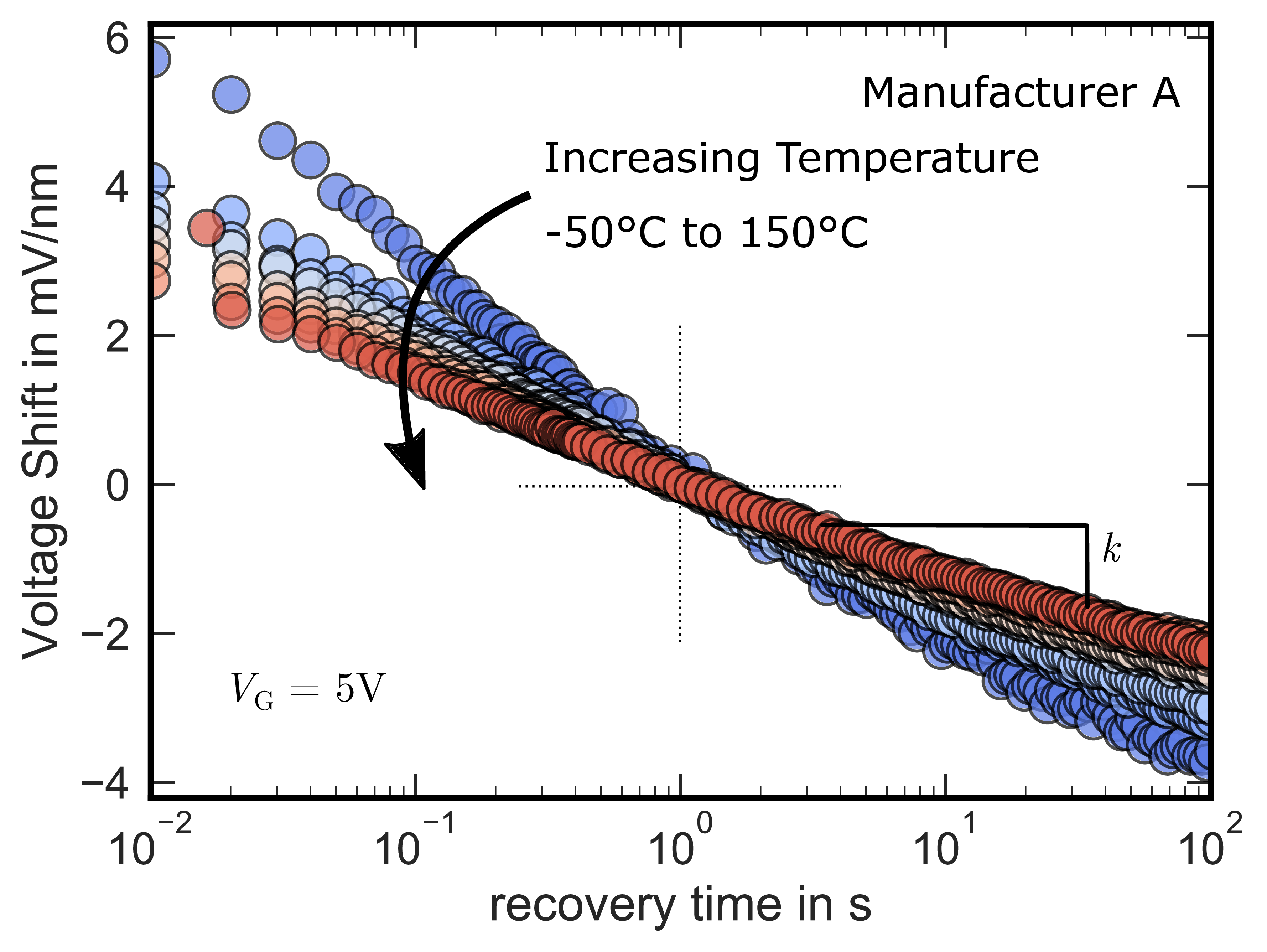
Figure 3.5: Temperature dependence of the recovery at after the 25 V positive bias stress for
100 s (device A). The recovery slope decreases with increasing temperature. The same trend is observed for all devices. This outcome indicates that most of the recovery already occurs within the first 10 ms after the
end of the stress pulse.
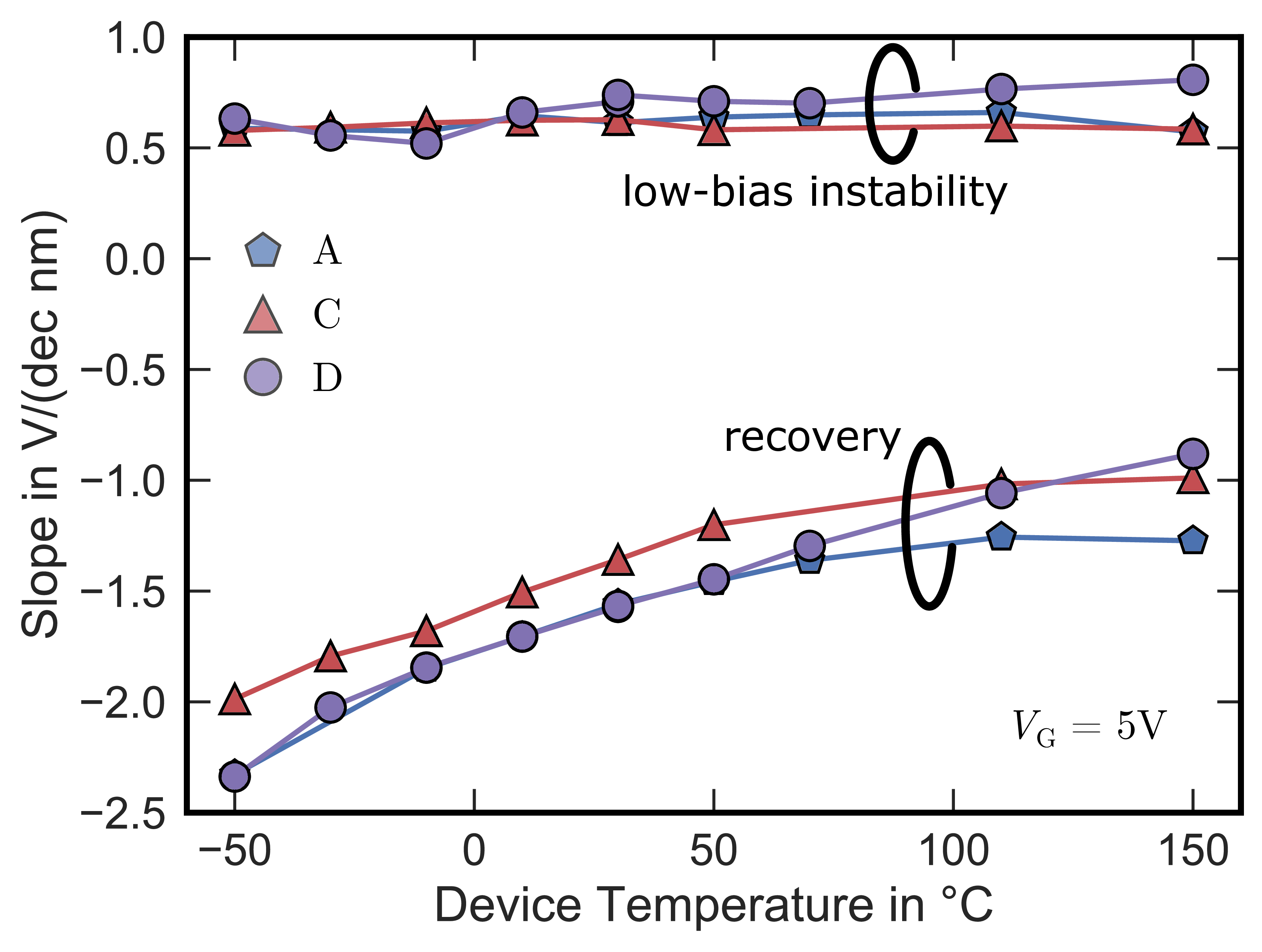
Figure 3.6: Temperature dependence of devices A, C and D. The slopes of the low-bias instability at 5 V stay nearly constant in the measured temperature range between −50 °C and 150 °C
at about 0.65 mV/dec/nm for all devices. The slope of the recovery traces increases with decreasing
temperature indicating the majority of carrier detrapping occurs within 10 ms after the end of the stress pulse.
mV/dec/nm for all devices. The slope of the recovery traces increases with decreasing
temperature indicating the majority of carrier detrapping occurs within 10 ms after the end of the stress pulse.
A comparison of the recovery and low-bias instability slopes of the devices A, C and D is shown in Fig. 3.6 indicating
temperature independent low-bias instability and increasing recovery slope with decreasing temperature for all devices. Although the devices from different manufactures differ in the absolute values of the threshold voltage shift, the
similar tendencies of all traces indicate that all observed instabilities are likely a fundamental physical
property of the SiC/SiO2 system and not related to, e.g. mobile ion contamination, fundamental differences in device processing, chip-package interaction or other issues. It is furthermore important to state that, unlike
in silicon devices, most of the does not originate from a permanent damage of
the interface (e.g. H-bond breakage) and is nearly fully recoverable, as will be shown in Section 3.3.
3.2.5 Summary
All SiC-MOSFET available on the market show nearly identical threshold voltage instabilities caused by trapping and detrapping of charges in oxide or near interface traps. The trapping/detrapping effect appears to be a fundamental property of the SiC/SiO2 system. As opposed to commercially available silicon-based MOSFETs, even an operation at low constant bias close to the threshold voltage causes a threshold voltage shift in the range of tens of millivolts. However, the actual mechanism causing the majority of the voltage shift in SiC devices differs from silicon and does not cause a permanent damage to the interface. The more pronounced trapping in the SiC/SiO2 system is likely a consequence of the different energetic positions of the 4H-SiC conduction and valence band edges allowing for a wider range of carrier exchange with traps near the SiC/SiO2 interface [37].
« PreviousUpNext »ContentsPrevious: 3 On the second Component: Bias Temperature Instability Top: 3 On the second Component: Bias Temperature Instability Next: 3.3 Preconditioned BTI measurements