|
Strained Si material has emerged as a strong contender for developing
transistors for the next generation electronics. Strain lifts the
degeneracy of
the valence and conduction bands which can be used to deliver superior
transport properties in comparison to bulk Si. The effect of strain on
device
characteristics can be studied using the Monte Carlo method. Based on Monte
Carlo simulations, a comprehensive set of models for the strained Si/SiGe
material system can be obtained. These models are to be implemented in a
device simulator and then used to investigate and design different strained Si
device structures.
An analytical model has been developed to describe the anisotropy of the
low-field electron mobility in strained Si on arbitrarily oriented SiGe
substrate. The model includes valley splitting for a given strain
tensor, the
effect of reduced inter-valley scattering with increasing splitting, and
doping
and temperature dependence. In order to validate the model, Monte Carlo
simulations were performed and the results obtained were fit to the
experimental data, available mainly in the form of piezo-resistance
coefficients. It was observed that changing the deformation potential
gave good
agreement with piezo-resistance-based mobility for low strain levels, whereas
adjusting the inter- and intra-valley coupling constants delivered the
desired
mobility enhancement.
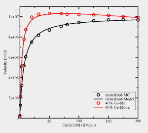
The electron high-field transport in strained Si has also been studied using
Full Band Monte Carlo simulations. From Monte Carlo simulations, it was
observed that the valley velocities decrease with an increase in strain,
whereas the total velocity increases. This phenomenon can be explained
by the
repopulation of valleys induced by the field. The total velocity also
shows a
region of small negative differential resistance (Gunn effect). Two
different
modeling approaches capturing these velocity-field characteristics have been
developed. The first one is based on calculating the total velocity from the
valley-specific electron velocities and populations, while the second is a
direct fit to the total velocity. Future work will concentrate on
modeling of
the various parameters for this material system based on Monte Carlo
results,
with special focus on the surface mobility and obtaining device
characteristics.
|