|
In integrated circuits, interfering signals can drive bipolar configurations
into snapback and this results in high current densities that may cause
damage. Due to the increasing density of devices and the integration of several
functional blocks with different power domains on a single chip, the presence
of parasitic bipolar configurations that can be driven into snapback has to be
taken into account. Automotive systems are an important application area in which it is necessary to consider this effect. These systems are often exposed to
high energetic interfering signals, on both supply and data lines, that may
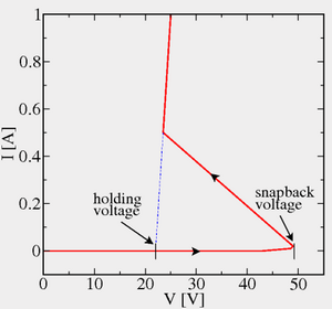
force the device into snapback. As long as the driving voltage lies above the
snapback holding voltage, the current density remains high and the destruction
process goes on and will cause damage to the device. To avoid this
self-destruction process, the goal in designing integrated circuits is
therefore to keep this snapback holding voltage of parasitic bipolar
configurations high, at least above the supply voltage. To keep this
structure from being driven into snapback, the snapback voltage itself lies in
the best case above the highest possible voltage that results from interfering
signals.
The snapback effect is not always an unwanted operating condition. It can be
systematically utilized as an ESD protection mechanism. Therefore a lateral
n-p-n structure of a gate-grounded MOSFET near the input contact is driven into
snapback during an ESD stress. In this application, the design goal is not to
keep the snapback holding voltage higher than the supply voltage. Instead, it
has to be low to keep the maximum local power dissipation resulting from the
current through the protection device low. The behavior of the protection
device going into snapback is primarily given by the snapback voltage, and it
must be assured that the protection circuit is driven into snapback before
there may be any damage to the protected circuit.
In both cases the snapback effect influences the reliability of integrated circuits. Simulation of this snapback phenomenon allows design decisions to be made to adapt the different characteristic values with the goal of increasing overall reliability. Simulation allows the consequences
of changing doping profiles, the shape of the p- or n-wells or the distances
between well borders and contacts to be investigated. This allows the snapback holding
voltage and the breakdown voltage itself to be adjusted and dynamic and
thermal aspects to be involved in the design. Considering these results in the design of
future smart power devices helps to improve the overall reliability.
|