|
While logical CMOS devices feature dielectric thicknesses below 1.2 nm,
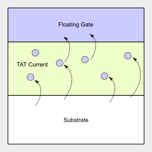
non-volatile memory cells rely on tunneling oxides as thick as 7 nm. In order
to speed up the programming and erasing process, strong electric fields are
applied across the dielectric. Due to the repeated high-field stress, trap
centers in the insulator are created which lead to trap-assisted tunneling at
low bias, forming stress-induced leakage current (SILC).
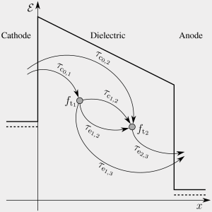
Modeling this gate leakage current for such devices is of paramount interest,
because it determines the retention time. Thicker dielectrics subject to high
field stress may have a high defect density. Thus not only direct tunneling but
also trap-assisted tunneling (TAT) currents play an important role. The
trap-assisted current component has been found to stem from inelastic tunneling
assisted by phonon emission.
The implementation of adequate models in the device simulator Minimos-NT
allows the simulation of the effect on the threshold voltage of memory devices and
therefore allows the extraction of the retention time.
In the simulation of degradation mechanisms of p-type LDMOS structures,
negative bias temperature instability (NBTI) can play an important role. It
leads to a rapid shift of transistor parameters like the threshold voltage
or the saturation current. For modeling NBTI the reaction-diffusion model is
established. The model predicts the generation of interface traps at the
silicon/silicon-dioxide interface by release of hydrogen atoms. The hydrogen
then diffuses into the oxide. By implementing a range of NBTI models in
Minimos-NT, this type of degradation of LDMOS structures can be studied in
detail.
|