|
Simulation and, therefore, optimization become increasingly more
time-consuming, especially if three-dimensional structures are considered.
Since current workstations offer increased performance at steadily decreasing
costs, they can easily be included as computational nodes in existing simulation
and optimization clusters. This allows the use of genetic optimization
algorithms, which are normally very time-consuming.
However, these new approaches require reliable tools that are able to
manage the
available network resources efficiently and avoid inconsistencies and
overloads
of certain simulation nodes. Therefore, the integrated simulation and
optimization framework SIESTA (Simulation Environment for Semiconductor
Technology Analysis) has been developed at the Institute for
Microelectronics.
It integrates a global network resource management and a variety of
optimizers
and simulators to combine the advantages of optimization strategies like
those
of gradient-based and genetic optimizers. This loosely-coupled system places
only minor restrictions on the external software tools.
Additionally,
fault tolerance has been included in the interface structures to guarantee a
stable operation.
With this variety of tools, the capabilities of the simulation framework
SIESTA
include investigations and optimizations of parameters for semiconductor
process
and device simulation. Furthermore, this framework supports inverse
modeling of
devices and technological processes, which is useful for the extraction of
specific
material and process parameters. The required information includes
measured data
and an appropriate base model which allows SIESTA to optimize the chosen
parameters automatically. This technique has already produced excellent
results
in process and device optimizations.
Currently, thermal effects in polycrystalline semiconductors and
complex-layered
interconnect structures are being investigated. The three-dimensional
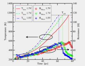
interconnect simulator STAP is used to predict critical temperatures in some
parts of the semiconductor as shown in the upper figure. At high
temperatures,
however, conventional models do not predict the change of the electrical
behavior correctly. Therefore it is necessary to include advanced models in
device simulators which are valid in these temperature ranges. SIESTA can be
used to calibrate analytical models included in device and circuit
simulators.
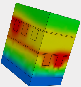
With well-calibrated models the investigation can also be focused on
complex-layered interconnect structures. The temperature distribution as a
result of a three-dimensional transient electro-thermal simulation with
STAP is
shown in the lower figure, which depicts two heated lines and the result of the
fast heat flow through several materials.
|