|
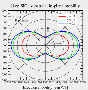
Development of a TCAD-ready, analytical electron mobility model for strained bulk Si
and low electric field has been completed. The model includes doping
dependence, temperature dependence, substrate orientation dependence
and dependence on the field direction. An analytical model for
electron velocity saturation at high fields has been developed and
fitted to full-band Monte Carlo results for strained Si.
Two approaches have been pursued, namely a three-valley model taking into account
valley population as internal variables, and a more empirical, direct
fit of the velocity-versus-field curve. A widely used high-field mobility
model has been augmented, and the dependences of all parameters on the
valley splitting are described by simple, analytical expressions.
The physical effects of electron transport in strained Si channels have
been studied in detail. Energy-resolved velocity profiles are a suitable
means to demonstrate effects of degenerate statistics, surface roughness
scattering, and screening on the surface mobility. As already observed
by other authors, the theoretically predicted mobility enhancement at
high normal field is still too small in comparison with measurement data.
A project on the modeling of silicon multi-gate FETs near the scaling limit
based on the Wigner equation has been continued. Inclusion of size
quantization of the carrier motion into the Wigner function approach
has been addressed in detail. It has been shown that an approach
treating size quantization directly within the Wigner function
formalism leads to a complicated set of integro-differential
equations for complex valued quantities, which could hardly be handled
without introduction of additional, restrictive approximations.
A practical approach which was found to be applicable to MOSFET
simulation is based on the separation of the quantized motion in
transverse direction from the motion in the direction of propagation.
In this case the eigen-energy depends on the position along the
propagating direction and plays the role of the coordinate-dependent
subband minimum. The electron motion within
each subband is then described by the corresponding Wigner equation,
with the potential energy determined by the
corresponding quantization energy of the transverse motion. The
subband decomposition has been shown to provide a good approximation
for double-gate and triple-gate silicon-on-insulator FETs. To prove
this, we expanded the density matrix in the subband-related basis set
and explicitly found the inter-subband coupling Hamiltonian. The
inter-subband coupling elements were computed for different FET
geometries and found to be much smaller than inter-subband energy,
which allows them to be safely neglected in practically relevant cases. An
existing numerical Monte Carlo simulator for solving the Wigner
equation has been extended and tested. Special attention was paid to
ultra-scaled devices in which the potential in the transport direction
along the channel changes quite rapidly, and tunneling through the
barrier is becoming important. Numerical stability of the simulation
method is improved by a spectral separation of the
potential along the channel into a classical and quantum mechanical
part. The classical potential accommodates the voltage
applied to the structure. The proposed potential separation allows
Wigner function-based simulations of practically relevant double-gate
SOI FETs.
Various architectures of carbon nanotube (CNT) FETs have been studied
using Minimos-NT. Assuming ballistic transport, a Schroedinger solver
coupled with the three-dimensional Poisson solver of Minimos-NT
is used to analyze both Schottky-type and ohmic-type CNT-FETs.
The current is calculated using the Landauer-Buettiker formula or
by solving the Schroedinger equation with open boundary conditions.
The charge on the tube is taken into account self-consistently.
To optimize the off-state characteristics of the CNT-FET, a dual-gate
structure has been proposed. The second gate effectively suppresses
hole tunneling at the drain contact. The dynamic response of CNT-FETs
has been analyzed employing the quasi-static approximation.
It has been shown that through appropriate selection of the gate-drain
spacer both the DC and AC response of ohmic contact CNT-FETs are improved.
Through an increase in the gate-drain spacer the ambipolar behavior is
suppressed and the parasitic capacitance between the gate and drain
contacts is reduced. Suppressing the ambipolar behavior increases the
on-to-off current ratio by three-orders of magnitude. Reducing the
parasitic capacitances increases the cutoff frequency about 30%.
The theory and practice of conjugated pi-electron systems and their
simulation by three-dimensional networks of energetically disordered
localized states has been studied. Amorphous and polycrystalline
zinc-phtalocyanine (ZnPc) samples at different doping levels have
been adopted as appropriate compounds for the development of a dynamic
Monte Carlo simulator covering diffusion and recombination phenomena in
carbon-based semiconductors. The extremely low intrinsic
conductivity can effectively be enhanced by p-doping, achieved by
co-evaporation with tetrafluoro-tetracyano-quinidimethane (F4-TCNQ).
A Gaussian disorder model has been implemented with an Abrahams-Miller-like
jumping rate, ignoring polaronic effects and tacitly assuming the polymer's
coupling to a heat bath. The ability to study the interplay between the
spatial and the energetic disorder for various molecules and crystallographic
phases has been considered to be an important feature
of the simulator. As a basic discretization principle, two-level
jumping sites, capable of simultaneously holding 2 LUMO and 2
HOMO-electrons (exclusion principle), repulsive on-level Coulomb
interaction (Hubbard-model-like) and an excitonic binding energy are
at this time implemented as the basic building blocks for the
molecular orbitals. A second activity is the extension of a
drift-diffusion-based device simulator with respect to organic
devices such as OFETs and OLEDs. For several parameters specific
models are required, such as mobility, density of states, trap
distribution, and band alignment. Various models for the mobility in organic semiconductors exist in literature. Currently,
a model based on the variable range hopping theory of Vissenberg is being
investigated in more detail. The model should cover a wide range of
temperatures and field strengths. Effects at the contacts play an important
role. Contact models including thermionic emission, tunneling and
interface recombination are implemented.
|