|
Ion implantation is the primary technology to introduce dopant atoms into
semiconductor wafers to form highly integrated CMOS devices, for instance,
System-on-a-Chip (SoC) devices which combine logic and memory consisting
of over 100 million transistors packed on a single silicon chip.
There are two dominant methods, global and local stress, for introducing
strain in the silicon channel. Research on biaxial tensile strained silicon
on relaxed SiGe has demonstrated that a larger improvement in mobility is
obtained by this global stress technique than for local stress techniques
(J.L. Hoyt, MIT). The formation of highly conductive ultra-shallow
source/drain extension junctions is one of the key challenges for the
processing of deep sub-100nm strained silicon CMOS devices. The capability
of accurately predicting doping profiles in the low energy regime by Monte
Carlo implantation tools can help to reduce the development time for such
a new CMOS technology.
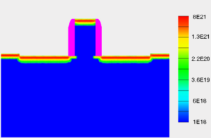
The Monte Carlo ion implantation simulator MCIMPL-II is an object-oriented,
multi-dimensional simulator, embedded in a process simulation environment.
The simulator is based on a binary collision approximation (BCA) and can
handle three-dimensional device structures consisting of amorphous and
crystalline materials including SiGe alloys of arbitrary germanium fraction.
For silicon layers with a thickness smaller than the critical thickness,
grown on a relaxed SiGe buffer layer, the horizontal lattice constant of
the strained silicon crystal is equal to that of the SiGe crystal, and the
vertical lattice constant can accurately be calculated by using the elastic
theory. We found that the arsenic distribution in strained silicon shows a
slightly deeper penetration compared to unstrained silicon, due to the
strain-induced volume dilation.
Negative bias temperature instability (NBTI) has emerged as the dominant
reliability concern for advanced CMOS devices. NBTI leads to a rapid shift
of the p-MOSFET parameters (threshold voltage, saturation current) due to
the generation of interface traps. Various stress experiments were performed
in order to investigate the NBTI degradation behavior for a 90nm CMOS
technology. The reaction-diffusion (R-D) model after M.A. Alam (IEDM 2003)
was used to analyze the NBTI phenomenon by diffusion of released hydrogen
in the gate oxide. A one-dimensional finite differences method was applied
for the discretization of the differential equations. The gate voltage and
frequency dependence of NBTI were included by means of an empirical
relationship. This simulation approach allows estimate of the p-MOSFET
lifetime, which depends strongly on the applied stress operation conditions.
|